Electrical Characteristics
MC9S12G Family Reference Manual Rev.1.27
NXP Semiconductors 1185
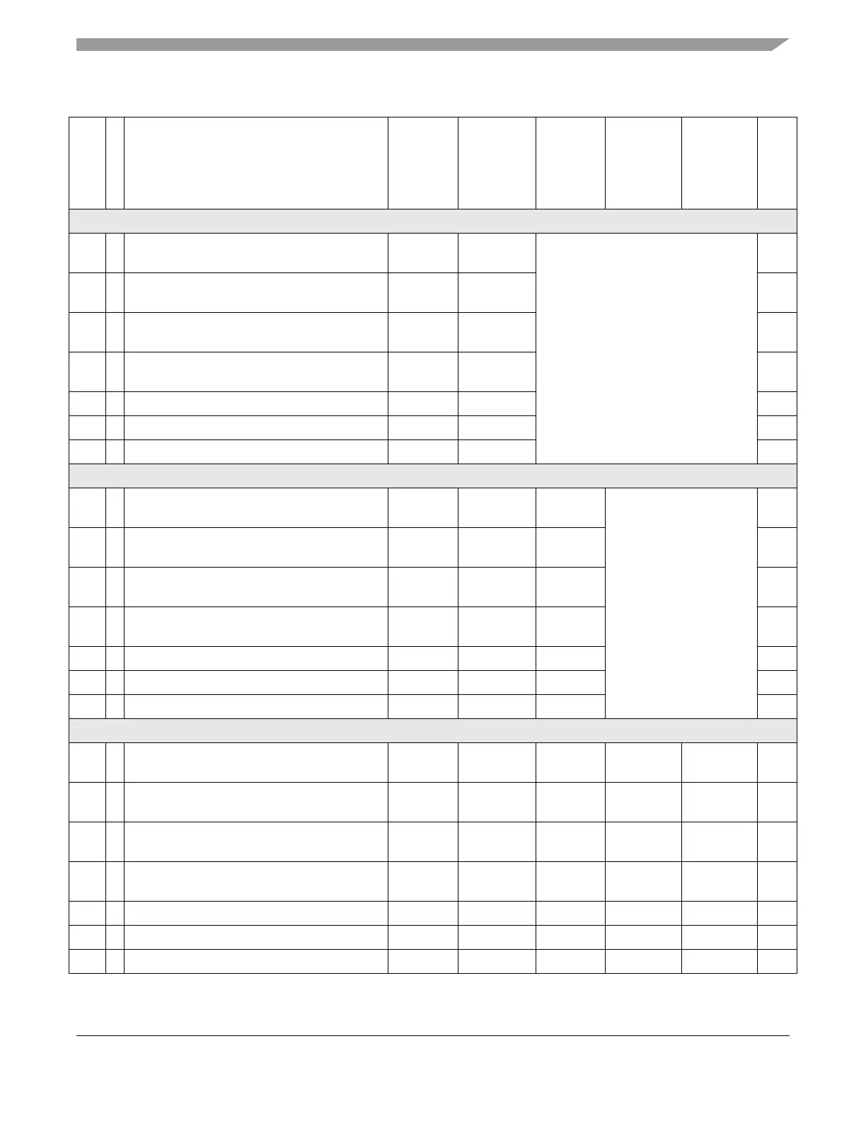
Table A-5. Thermal Package Characteristics
1
Num C Rating Symbol
S12GN32,
S12GNA32,
S12GN16,
S12GNA16
S12G64,
S12GA64,
S12G48,
S12GN48,
S12GA64
S12G128,
S12GA128,
S12G96,
S12GA96
S12G240,
S12GA240,
S12G192,
S12GA192
Unit
20-pin TSSOP
1D
Thermal resistance single sided PCB,
natural convection
2
JA
91 C/W
2D
Thermal resistance single sided PCB
@ 200 ft/min
3
JMA
72 C/W
3D
Thermal resistance double sided PCB
with 2 internal planes, natural convection
3
JA
58 C/W
4D
Thermal resistance double sided PCB
with 2 internal planes @ 200 ft/min
3
JMA
51 C/W
5 D Junction to Board
4
JB
29 C/W
6 D Junction to Case
5
JC
20 C/W
7 D Junction to Package Top
6
JT
4 C/W
32-pin LQFP
8D
Thermal resistance single sided PCB,
natural convection
2
JA
81 84 C/W
9D
Thermal resistance single sided PCB
@ 200 ft/min
3
JMA
68 70 C/W
10 D
Thermal resistance double sided PCB
with 2 internal planes, natural convection
3
JA
57 56 C/W
11 D
Thermal resistance double sided PCB
with 2 internal planes @ 200 ft/min
3
JMA
50 49 C/W
12 D Junction to Board
4
JB
35 32 C/W
13 D Junction to Case
5
JC
25 23 C/W
14 D Junction to Package Top
6
JT
86 C/W
48-pin LQFP
15 D
Thermal resistance single sided PCB,
natural convection
2
JA
81 80 79 75 C/W
16 D
Thermal resistance single sided PCB
@ 200 ft/min
3
JMA
68 67 66 62 C/W
17 D
Thermal resistance double sided PCB
with 2 internal planes, natural convection
3
JA
57 56 56 51 C/W
18 D
Thermal resistance double sided PCB
with 2 internal planes @ 200 ft/min
3
JMA
50 50 49 45 C/W
19 D Junction to Board
4
JB
35 34 33 30 C/W
20 D Junction to Case
5
JC
25 24 21 19 C/W
21 D Junction to Package Top
6
JT
864N/AC/W

 Loading...


