Port Integration Module (S12GPIMV1)
MC9S12G Family Reference Manual Rev.1.27
218 NXP Semiconductors
2.4.3.31 Port M Polarity Select Register (PPSM)
2.4.3.32 Port M Wired-Or Mode Register (WOMM)
Address 0x0255 (G1, G2) Access: User read/write
1
1
Read: Anytime
Write: Anytime
76543210
R0000
PPSM3 PPSM2 PPSM1 PPSM0
W
Reset00000000
Address 0x0255 (G3) Access: User read/write
1
76543210
R000000
PPSM1 PPSM0
W
Reset00000000
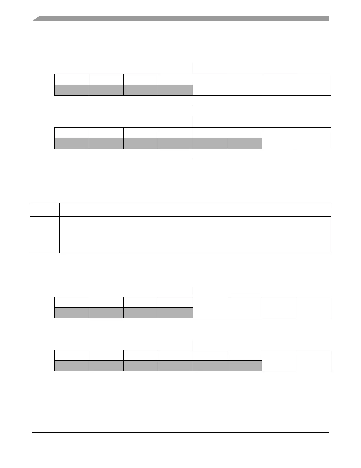
Figure 2-32. Port M Polarity Select Register (PPSM)
Table 2-56. PPSM Register Field Descriptions
Field Description
3-0
PPSM
Port M pull device select—Configure pull device polarity on input pin
This bit selects a pullup or a pulldown device if enabled on the associated port input pin.
1 Pulldown device selected
0 Pullup device selected
Address 0x0256 (G1, G2) Access: User read/write
1
1
Read: Anytime
Write: Anytime
76543210
R0000
WOMM3 WOMM2 WOMM1 WOMM0
W
Reset00000000
Address 0x0256 (G3) Access: User read/write
1
76543210
R000000
WOMM1 WOMM0
W
Reset00000000
Figure 2-33. Port M Wired-Or Mode Register (WOMM)

 Loading...


