Background Debug Module (S12SBDMV1)
MC9S12G Family Reference Manual Rev.1.27
NXP Semiconductors 295
Figure 7-8. BDM Target-to-Host Serial Bit Timing (Logic 1)
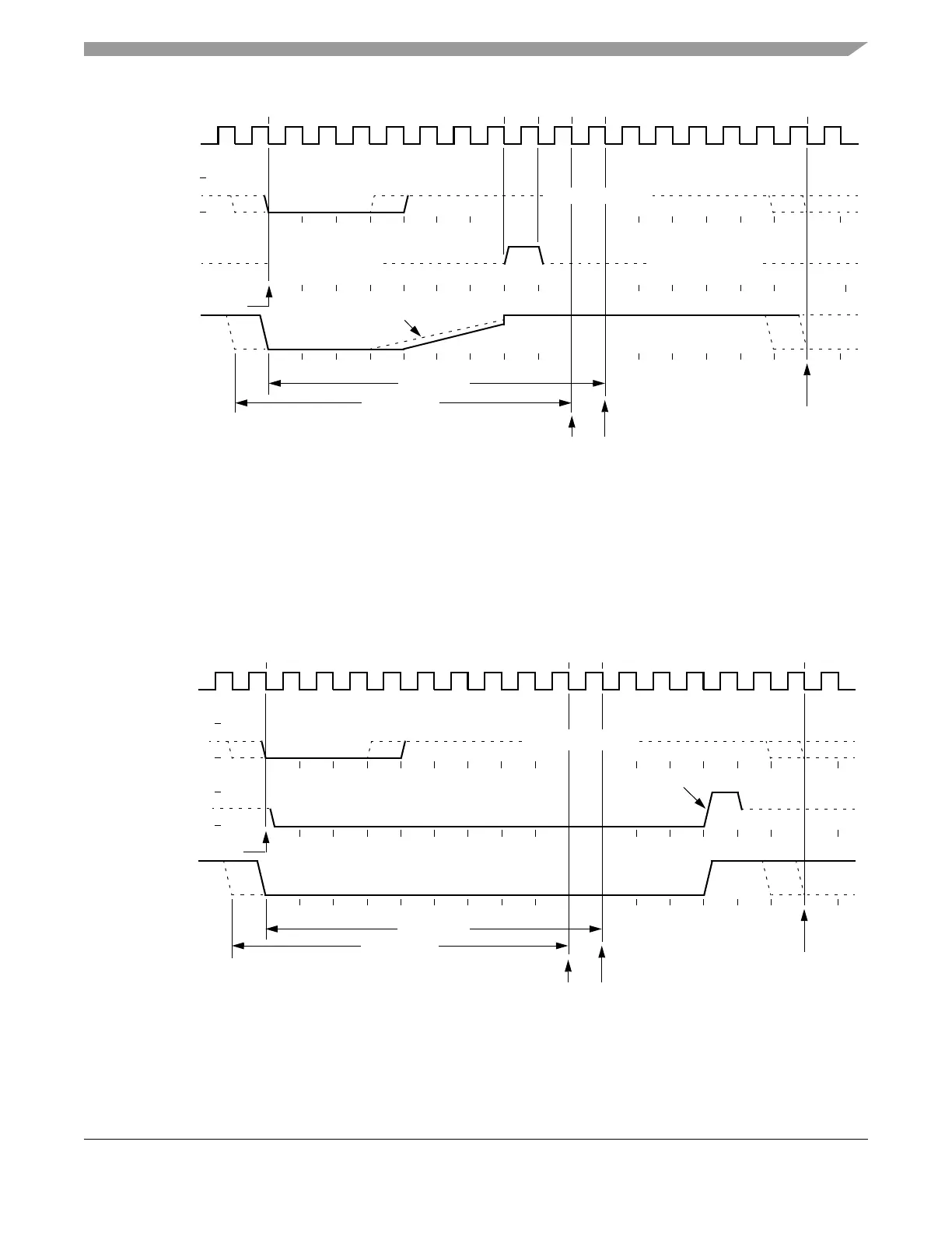
Figure 7-9 shows the host receiving a logic 0 from the target. Since the host is asynchronous to the target,
there is up to a one clock-cycle delay from the host-generated falling edge on BKGD to the start of the bit
time as perceived by the target. The host initiates the bit time but the target finishes it. Since the target
wants the host to receive a logic 0, it drives the BKGD pin low for 13 target clock cycles then briefly drives
it high to speed up the rising edge. The host samples the bit level about 10 target clock cycles after starting
the bit time.
Figure 7-9. BDM Target-to-Host Serial Bit Timing (Logic 0)
High-Impedance
Earliest
Start of
Next Bit
R-C Rise
10 Cycles
10 Cycles
Host Samples
BKGD Pin
Perceived
Start of Bit Time
BKGD Pin
BDM Clock
(Target MCU)
Host
Drive to
BKGD Pin
Target System
Speedup
Pulse
High-Impedance
High-Impedance
Earliest
Start of
Next Bit
BDM Clock
(Target MCU)
Host
Drive to
BKGD Pin
BKGD Pin
Perceived
Start of Bit Time
10 Cycles
10 Cycles
Host Samples
BKGD Pin
Target System
Drive and
Speedup Pulse
Speedup Pulse
High-Impedance

 Loading...


