Device Overview MC9S12G-Family
MC9S12G Family Reference Manual Rev.1.27
NXP Semiconductors 41
NOTE
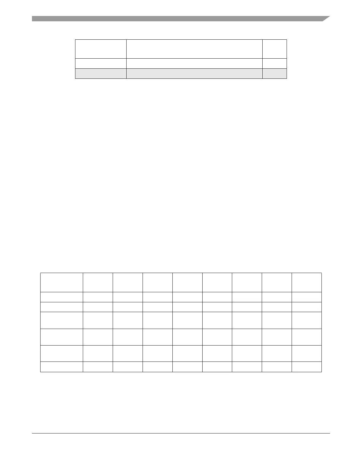
Reserved register space shown in Table 1-3 is not allocated to any module.
This register space is reserved for future use. Writing to these locations has
no effect. Read access to these locations returns zero.
Figure 1-2 shows S12G CPU and BDM local address translation to the global memory map as a graphical
representation. In conjunction Table 1-4 shows the address ranges and mapping to 256K global memory
space for P-Flash, EEPROM and RAM. The whole 256K global memory space is visible through the
P-Flash window located in the 64k local memory map located at 0x8000 - 0xBFFF using the PPAGE
register.
0x03C8–0x03CF DAC1 (Digital to Analog Converter)
8
8
0x03D0–0x03FF Reserved 48
1
The SCI1 is not available on the S12GN8, S12GN16, S12GN32, and S12GN32 devices
2
The SCI2 is not available on the S12GN8, S12GN16, S12GN32, S12GN32, S12G48,
and S12G64 devices
3
The SPI1 is not available on the S12GN8, S12GN16, S12GN24, and S12GN32 devices
4
The SPI2 is not available on the S12GN8, S12GN16, S12GN32, S12GN32, S12G48,
and S12G64 devices
5
The CAN is not available on the S12GN8, S12GN16, S12GN24, S12GN32, and
S12GN48 devices
6
The ACMP is only available on the S12GN8, S12GN16, S12GN24, S12GN32,
S12GN48,S12GN48, S12G48, and S12G64 devices
7
The RVA is only available on the S12GA192 and S12GA240 devices
8
DAC0 and DAC1 are only available on the S12GA192 and S12GA240 devices
Table 1-4. MC9S12G-Family Memory Parameters
Feature S12GN16 S12GN32
S12G48
S12GN48
S12G64 S12G96 S12G128
S12G192
S12GA192
S12G240
S12GA240
P-Flash size 16KB 32KB 48KB 64KB 96KB 128KB 192KB 240KB
PF_LOW 0x3C000 0x38000 0x34000 0x30000 0x28000 0x20000 0x10000 0x04000
PF_LOW_UNP
(unpaged)
1
0xC0000x80000x4000—————
PPAGES
0x0F
0x0E -
0x0F
0x0D -
0x0F
0x0C -
0x0F
0x0A -
0x0F
0x08 -
0x0F
0x04 -
0x0F
0x01 -
0x0F
EEPROM
[Bytes]
512 1024 1536 2048 3072 4096 4096 4096
EEPROM_HI 0x05FF 0x07FF 0x09FF 0x0BFF 0x0FFF 0x13FF 0x13FF 0x13FF
Address Module
Size
(Bytes)

 Loading...


