Analog-to-Digital Converter (ADC12B12CV2)
MC9S12G Family Reference Manual Rev.1.27
NXP Semiconductors 489
14.3.2.2 ATD Control Register 1 (ATDCTL1)
Writes to this register will abort current conversion sequence.
Read: Anytime
Write: Anytime
1
If only AN0 should be converted use MULT=0.
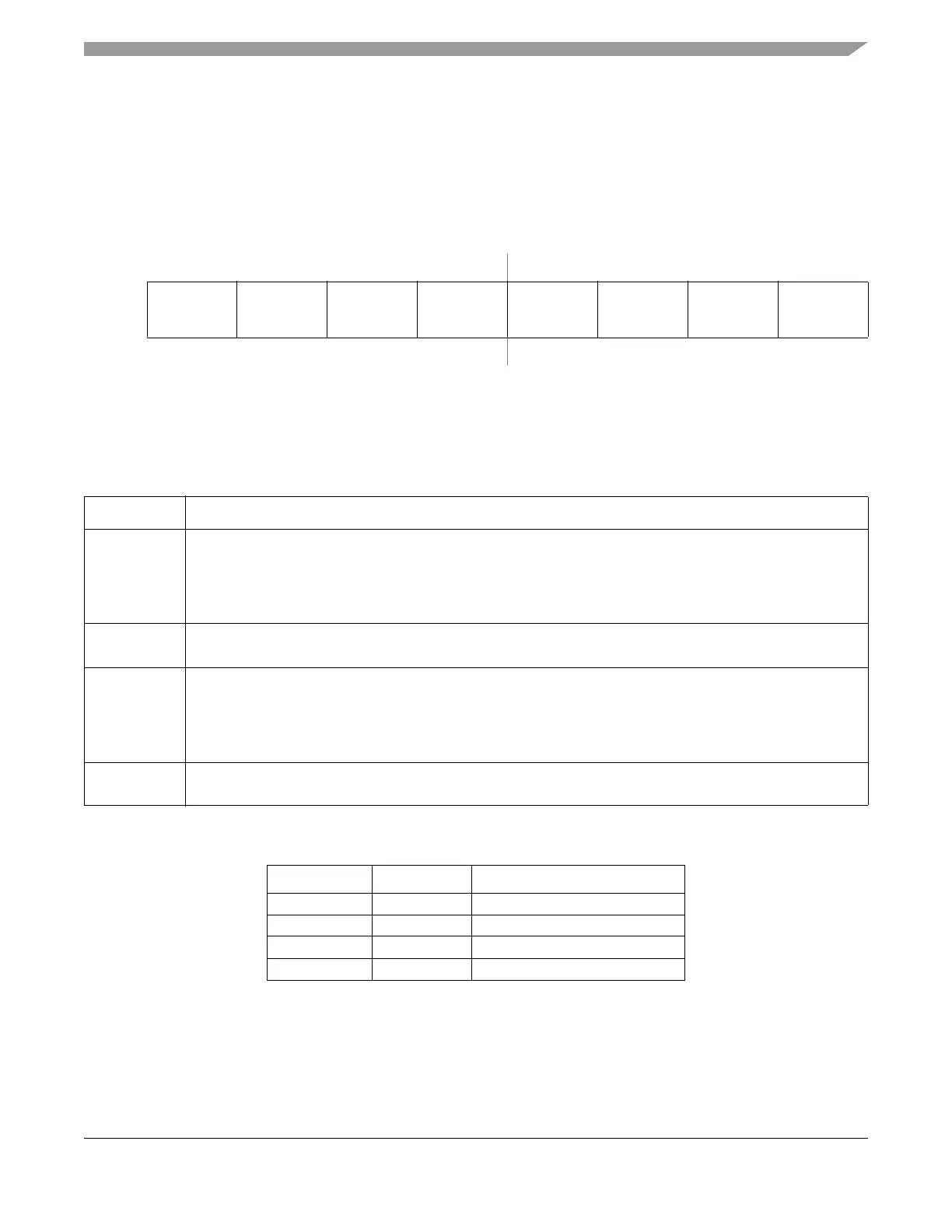
Module Base + 0x0001
76543210
R
ETRIGSEL SRES1 SRES0 SMP_DIS ETRIGCH3 ETRIGCH2 ETRIGCH1 ETRIGCH0
W
Reset00101111
Figure 14-4. ATD Control Register 1 (ATDCTL1)
Table 14-3. ATDCTL1 Field Descriptions
Field Description
7
ETRIGSEL
External Trigger Source Select — This bit selects the external trigger source to be either one of the AD
channels or one of the ETRIG3-0 inputs. See device specification for availability and connectivity of ETRIG3-0
inputs. If a particular ETRIG3-0 input option is not available, writing a 1 to ETRISEL only sets the bit but has
no effect, this means that one of the AD channels (selected by ETRIGCH3-0) is configured as the source for
external trigger. The coding is summarized in Table 14-5.
6–5
SRES[1:0]
A/D Resolution Select — These bits select the resolution of A/D conversion results. See Table 14-4 for
coding.
4
SMP_DIS
Discharge Before Sampling Bit
0 No discharge before sampling.
1 The internal sample capacitor is discharged before sampling the channel. This adds 2 ATD clock cycles to
the sampling time. This can help to detect an open circuit instead of measuring the previous sampled
channel.
3–0
ETRIGCH[3:0]
External Trigger Channel Select — These bits select one of the AD channels or one of the ETRIG3-0 inputs
as source for the external trigger. The coding is summarized in Table 14-5.
Table 14-4. A/D Resolution Coding
SRES1 SRES0 A/D Resolution
0 0 8-bit data
0 1 10-bit data
1 0 12-bit data
11 Reserved

 Loading...


