Pulse-Width Modulator (S12PWM8B8CV2)
MC9S12G Family Reference Manual Rev.1.27
NXP Semiconductors 641
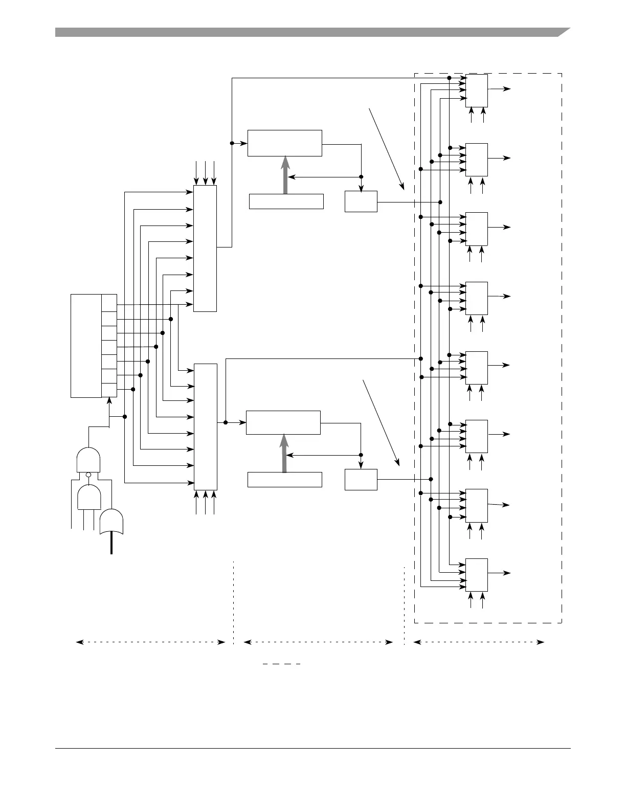
Figure 19-15. PWM Clock Select Block Diagram
128248163264
PCKB2
PCKB1
PCKB0
M
U
X
Clock A
Clock B
Clock SA
Clock A/2, A/4, A/6,....A/512
Prescale Scale
Divide by
PFRZ
Freeze Mode Signal
Bus Clock
Clock Select
M
U
X
Clock to
PWM Ch 0
M
U
X
Clock to
PWM Ch 2
M
U
X
Clock to
PWM Ch 1
M
U
X
Clock to
PWM Ch 4
M
U
X
Clock to
PWM Ch 5
M
U
X
Clock to
PWM Ch 6
M
U
X
Clock to
PWM Ch 7
M
U
X
Clock to
PWM Ch 3
Load
DIV 2PWMSCLB
Clock SB
Clock B/2, B/4, B/6,....B/512
M
U
X
PCKA2
PCKA1
PCKA0
PWME7-0
Count = 1
Load
DIV 2PWMSCLA
Count = 1
8-Bit Down
Counter
8-Bit Down
Counter
Prescaler Taps:
Maximum possible channels, scalable in pairs from PWM0 to PWM7.
PCLK0 PCLKAB0
PCLK1 PCLKAB1
PCLK7 PCLKAB7
PCLK6 PCLKAB6
PCLK5 PCLKAB5
PCLK4 PCLKAB4
PCLK3 PCLKAB3
PCLK2 PCLKAB2

 Loading...


