Pulse-Width Modulator (S12PWM8B8CV2)
MC9S12G Family Reference Manual Rev.1.27
646 NXP Semiconductors
NOTE
Changing the PWM output mode from left aligned to center aligned output
(or vice versa) while channels are operating can cause irregularities in the
PWM output. It is recommended to program the output mode before
enabling the PWM channel.
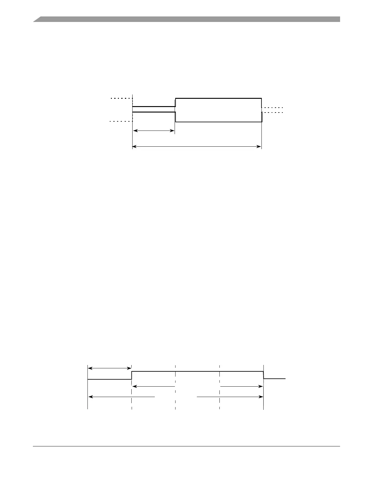
Figure 19-17. PWM Left Aligned Output Waveform
To calculate the output frequency in left aligned output mode for a particular channel, take the selected
clock source frequency for the channel (A, B, SA, or SB) and divide it by the value in the period register
for that channel.
• PWMx Frequency = Clock (A, B, SA, or SB) / PWMPERx
• PWMx Duty Cycle (high time as a% of period):
— Polarity = 0 (PPOLx = 0)
Duty Cycle = [(PWMPERx-PWMDTYx)/PWMPERx] * 100%
— Polarity = 1 (PPOLx = 1)
Duty Cycle = [PWMDTYx / PWMPERx] * 100%
As an example of a left aligned output, consider the following case:
Clock Source = E, where E = 10 MHz (100 ns period)
PPOLx = 0
PWMPERx = 4
PWMDTYx = 1
PWMx Frequency = 10 MHz/4 = 2.5 MHz
PWMx Period = 400 ns
PWMx Duty Cycle = 3/4 *100% = 75%
The output waveform generated is shown in Figure 19-18.
Figure 19-18. PWM Left Aligned Output Example Waveform
PWMDTYx
Period = PWMPERx
PPOLx = 0
PPOLx = 1
Period = 400 ns
E = 100 ns
Duty Cycle = 75%

 Loading...


