Timer Module (TIM16B6CV3)
MC9S12G Family Reference Manual Rev.1.27
728 NXP Semiconductors
22.3.2.8 Timer Interrupt Enable Register (TIE)
Read: Anytime
Write: Anytime.
22.3.2.9 Timer System Control Register 2 (TSCR2)
Read: Anytime
Write: Anytime.
1 1 Capture on any edge (rising or falling)
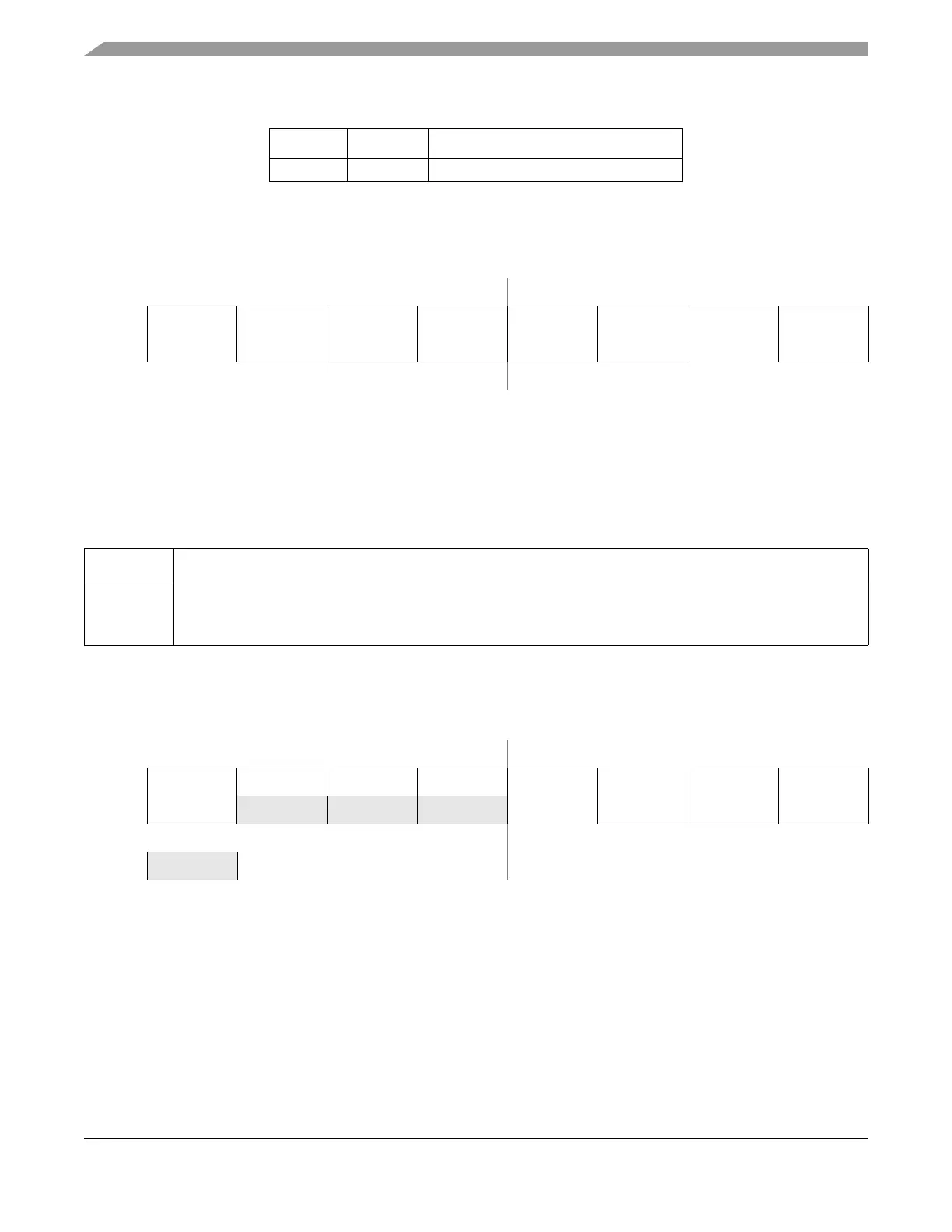
Module Base + 0x000C
76543210
R
RESERVED RESERVED C5I C4I C3I C2I C1I C0I
W
Reset00000000
Figure 22-14. Timer Interrupt Enable Register (TIE)
Table 22-10. TIE Field Descriptions
Note: Writing to unavailable bits has no effect. Reading from unavailable bits return a zero
Field Description
5:0
C5I:C0I
Input Capture/Output Compare “x” Interrupt Enable — The bits in TIE correspond bit-for-bit with the bits in
the TFLG1 status register. If cleared, the corresponding flag is disabled from causing a hardware interrupt. If set,
the corresponding flag is enabled to cause a interrupt.
Module Base + 0x000D
76543210
R
TOI
000
RESERVED PR2 PR1 PR0
W
Reset00000000
= Unimplemented or Reserved
Figure 22-15. Timer System Control Register 2 (TSCR2)
Table 22-9. Edge Detector Circuit Configuration
EDGnB EDGnA Configuration

 Loading...


