Timer Module (TIM16B6CV3)
MC9S12G Family Reference Manual Rev.1.27
NXP Semiconductors 727
22.3.2.7 Timer Control Register 3/Timer Control Register 4 (TCTL3 and TCTL4)
Read: Anytime
Write: Anytime.
Table 22-7. Compare Result Output Action
OMx OLx Action
0 0 No output compare
action on the timer output signal
0 1 Toggle OCx output line
1 0 Clear OCx output line to zero
1 1 Set OCx output line to one
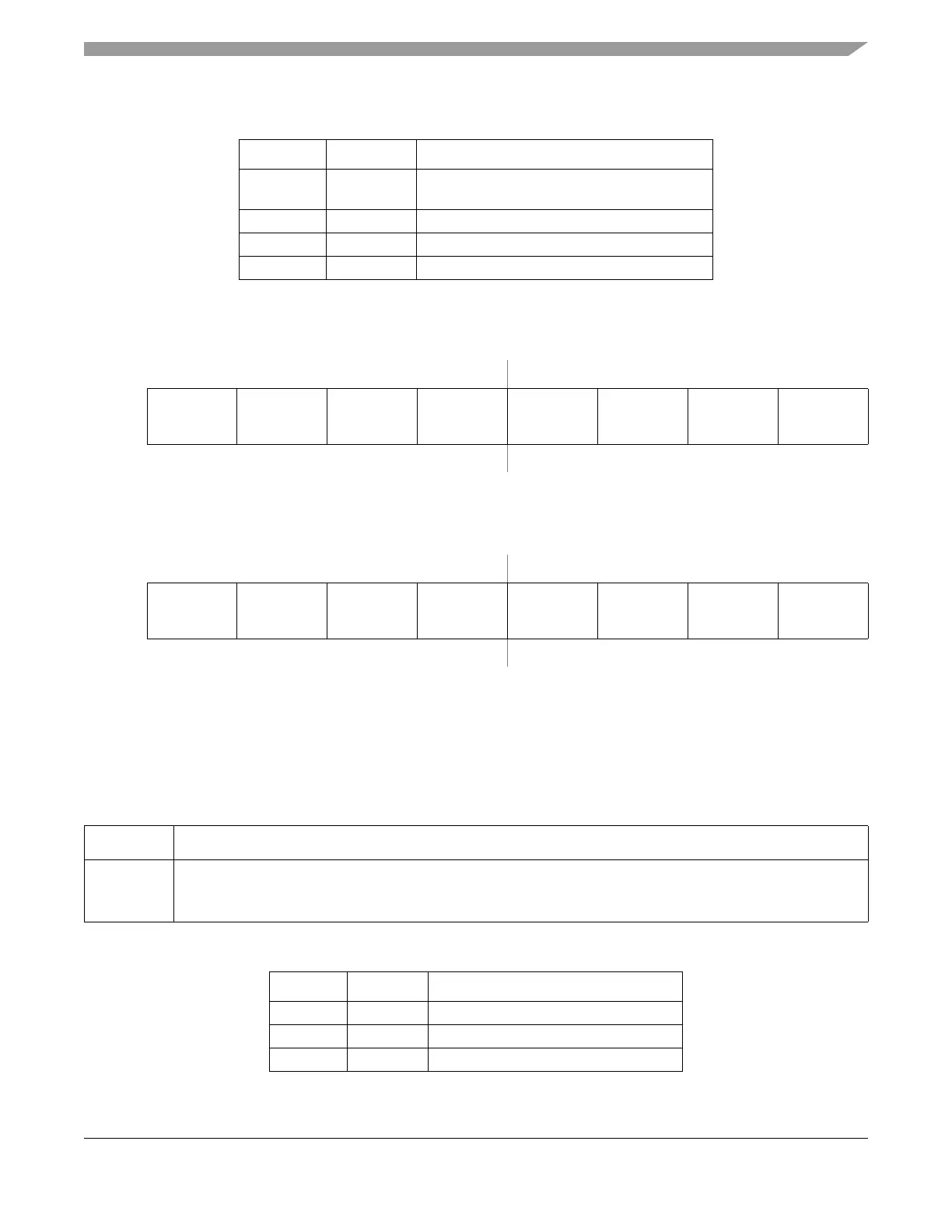
Module Base + 0x000A
76543210
R
RESERVED RESERVED RESERVED RESERVED EDG5B EDG5A EDG4B EDG4A
W
Reset00000000
Figure 22-12. Timer Control Register 3 (TCTL3)
Module Base + 0x000B
76543210
R
EDG3B EDG3A EDG2B EDG2A EDG1B EDG1A EDG0B EDG0A
W
Reset00000000
Figure 22-13. Timer Control Register 4 (TCTL4)
Table 22-8. TCTL3/TCTL4 Field Descriptions
Note: Writing to unavailable bits has no effect. Reading from unavailable bits return a zero.
Field Description
5:0
EDGnB
EDGnA
Input Capture Edge Control — These six pairs of control bits configure the input capture edge detector circuits.
Table 22-9. Edge Detector Circuit Configuration
EDGnB EDGnA Configuration
0 0 Capture disabled
0 1 Capture on rising edges only
1 0 Capture on falling edges only

 Loading...


