Timer Module (TIM16B6CV3)
MC9S12G Family Reference Manual Rev.1.27
NXP Semiconductors 731
22.3.2.12 Timer Input Capture/Output Compare Registers High and Low 0–
5(TCxH and TCxL)
1
This register is available only when the corresponding channel exists and is reserved if that channel does not exist. Writes to
a reserved register have no functional effect. Reads from a reserved register return zeroes.
Depending on the TIOS bit for the corresponding channel, these registers are used to latch the value of the
free-running counter when a defined transition is sensed by the corresponding input capture edge detector
or to trigger an output action for output compare.
Read: Anytime
Write: Anytime for output compare function.Writes to these registers have no meaning or effect during
input capture. All timer input capture/output compare registers are reset to 0x0000.
NOTE
Read/Write access in byte mode for high byte should take place before low
byte otherwise it will give a different result.
Module Base + 0x0010 = TC0H
0x0012 = TC1H
0x0014=TC2H
0x0016=TC3H
0x0018=TC4H
0x001A=TC5H
0x001C=RESERVD
0x001E=RESERVD
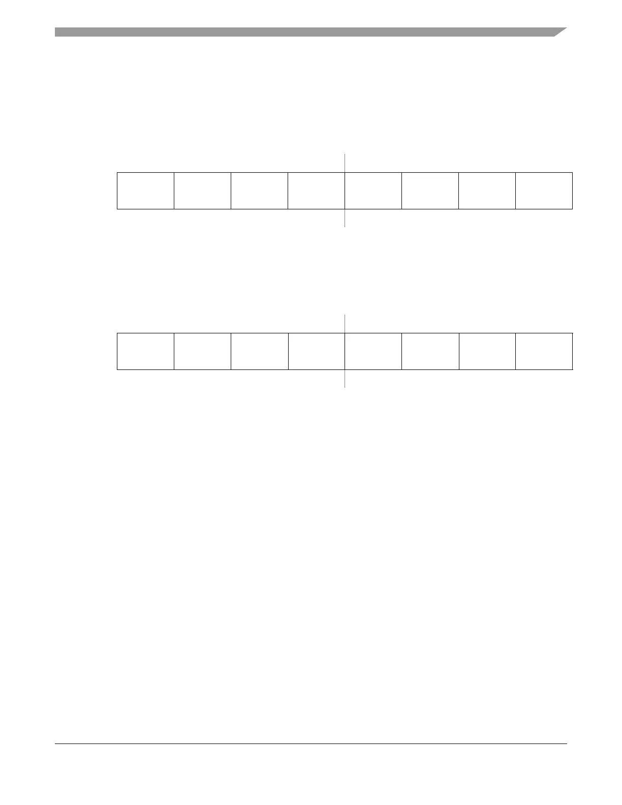
15 14 13 12 11 10 9 0
R
Bit 15 Bit 14 Bit 13 Bit 12 Bit 11 Bit 10 Bit 9 Bit 8
W
Reset00000000
Figure 22-18. Timer Input Capture/Output Compare Register x High (TCxH)
Module Base + 0x0011 = TC0L
0x0013 = TC1L
0x0015 =TC2L
0x0017=TC3L
0x0019 =TC4L
0x001B=TC5L
0x001D=RESERVD
0x001F=RESERVD
76543210
R
Bit 7Bit 6Bit 5Bit 4Bit 3Bit 2Bit 1Bit 0
W
Reset00000000
Figure 22-19. Timer Input Capture/Output Compare Register x Low (TCxL)

 Loading...


