Timer Module (TIM16B8CV3)
MC9S12G Family Reference Manual Rev.1.27
NXP Semiconductors 743
23.3.2.1 Timer Input Capture/Output Compare Select (TIOS)
Read: Anytime
Write: Anytime
0x0021
PAFLG
R000000
PAOVF PAIF
W
0x0022
PACNTH
R
PACNT15 PACNT14 PACNT13 PACNT12 PACNT11 PACNT10 PACNT9 PACNT8
W
0x0023
PACNTL
R
PACNT7 PACNT6 PACNT5 PACNT4 PACNT3 PACNT2 PACNT1 PACNT0
W
0x0024–0x002B
Reserved
R
W
0x002C
OCPD
R
OCPD7 OCPD6 OCPD5 OCPD4 OCPD3 OCPD2 OCPD1 OCPD0
W
0x002D
Reserved
R
0x002E
PTPSR
R
PTPS7 PTPS6 PTPS5 PTPS4 PTPS3 PTPS2 PTPS1 PTPS0
W
0x002F
Reserved
R
W
1
The register is available only if corresponding channel exists.
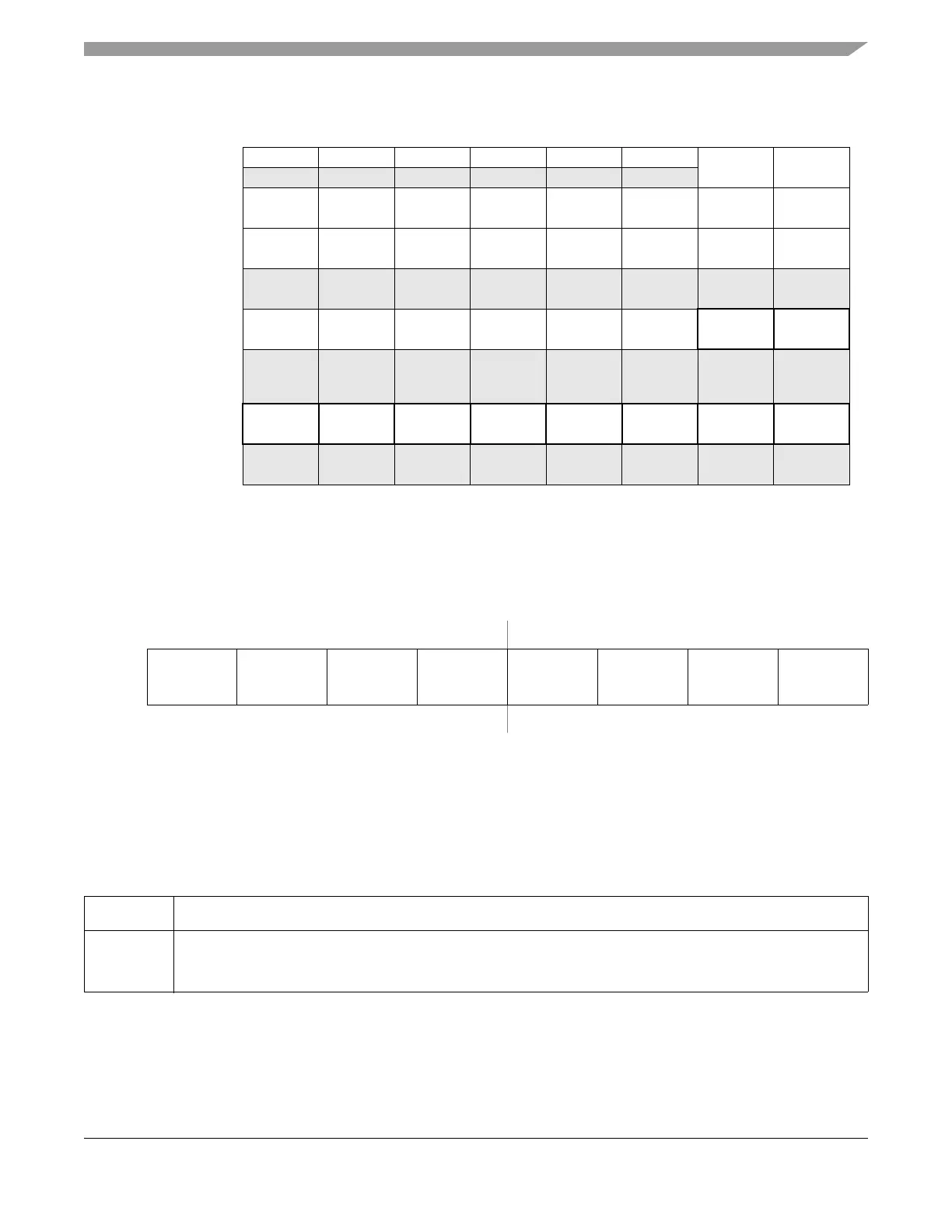
Module Base + 0x0000
76543210
R
IOS7 IOS6 IOS5 IOS4 IOS3 IOS2 IOS1 IOS0
W
Reset00000000
Figure 23-6. Timer Input Capture/Output Compare Select (TIOS)
Table 23-2. TIOS Field Descriptions
Note: Writing to unavailable bits has no effect. Reading from unavailable bits return a zero.
Field Description
7:0
IOS[7:0]
Input Capture or Output Compare Channel Configuration
0 The corresponding implemented channel acts as an input capture.
1 The corresponding implemented channel acts as an output compare.
Register
Name
Bit 76 5 4 3 2 1Bit 0
Figure 23-5. TIM16B8CV3 Register Summary (Sheet 2 of 2)

 Loading...


