Timer Module (TIM16B8CV3)
MC9S12G Family Reference Manual Rev.1.27
744 NXP Semiconductors
23.3.2.2 Timer Compare Force Register (CFORC)
Read: Anytime but will always return 0x0000 (1 state is transient)
Write: Anytime
23.3.2.3 Output Compare 7 Mask Register (OC7M)
Read: Anytime
Write: Anytime
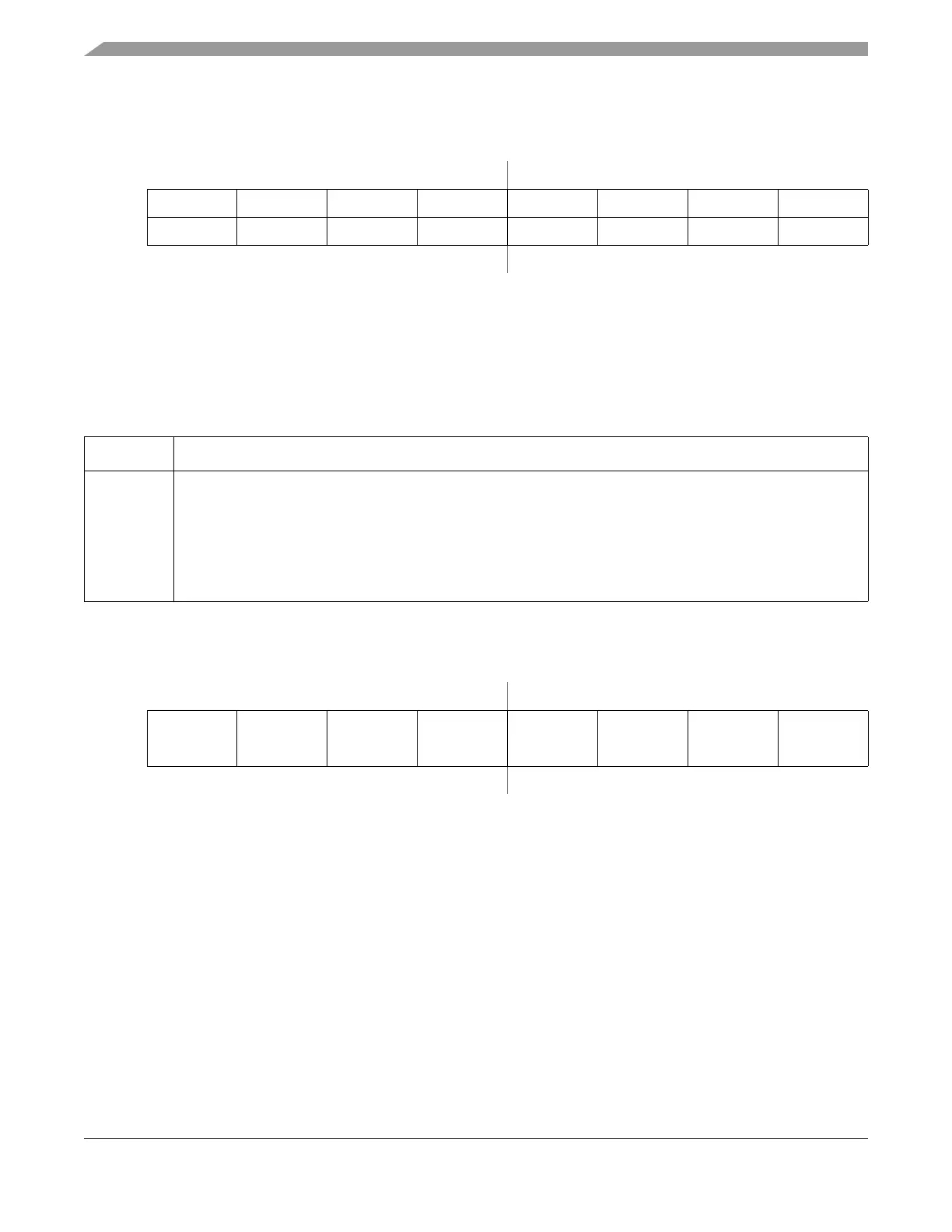
Module Base + 0x0001
76543210
R00000000
W FOC7 FOC6 FOC5 FOC4 FOC3 FOC2 FOC1 FOC0
Reset00000000
Figure 23-7. Timer Compare Force Register (CFORC)
Table 23-3. CFORC Field Descriptions
Note: Writing to unavailable bits has no effect. Reading from unavailable bits return a zero.
Field Description
7:0
FOC[7:0]
Note: Force Output Compare Action for Channel 7:0 — A write to this register with the corresponding data
bit(s) set causes the action which is programmed for output compare “x” to occur immediately. The action
taken is the same as if a successful comparison had just taken place with the TCx register except the
interrupt flag does not get set. A channel 7 event, which can be a counter overflow when TTOV[7] is set
or a successful output compare on channel 7, overrides any channel 6:0 compares. If forced output
compare on any channel occurs at the same time as the successful output compare then forced output
compare action will take precedence and interrupt flag won’t get set.
Module Base + 0x0002
76543210
R
OC7M7 OC7M6 OC7M5 OC7M4 OC7M3 OC7M2 OC7M1 OC7M0
W
Reset00000000
Figure 23-8. Output Compare 7 Mask Register (OC7M)

 Loading...


