Timer Module (TIM16B8CV3)
MC9S12G Family Reference Manual Rev.1.27
748 NXP Semiconductors
23.3.2.8 Timer Control Register 1/Timer Control Register 2 (TCTL1/TCTL2)
Read: Anytime
Write: Anytime
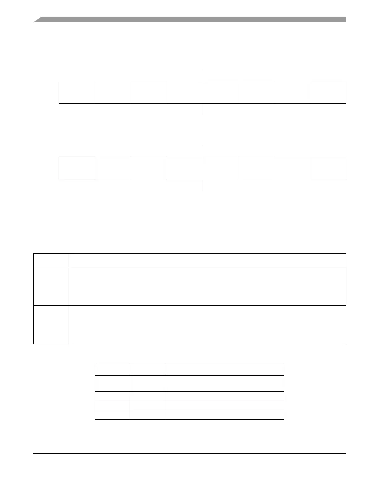
Module Base + 0x0008
76543210
R
OM7 OL7 OM6 OL6 OM5 OL5 OM4 OL4
W
Reset00000000
Figure 23-14. Timer Control Register 1 (TCTL1)
Module Base + 0x0009
76543210
R
OM3 OL3 OM2 OL2 OM1 OL1 OM0 OL0
W
Reset00000000
Figure 23-15. Timer Control Register 2 (TCTL2)
Table 23-8. TCTL1/TCTL2 Field Descriptions
Note: Writing to unavailable bits has no effect. Reading from unavailable bits return a zero
Field Description
7:0
OMx
Output Mode — These eight pairs of control bits are encoded to specify the output action to be taken as a result
of a successful OCx compare. When either OMx or OLx is 1, the pin associated with OCx becomes an output
tied to OCx.
Note: To enable output action by OMx bits on timer port, the corresponding bit in OC7M should be cleared. For
an output line to be driven by an OCx the OCPDx must be cleared.
7:0
OLx
Output Level — These eightpairs of control bits are encoded to specify the output action to be taken as a result
of a successful OCx compare. When either OMx or OLx is 1, the pin associated with OCx becomes an output
tied to OCx.
Note: To enable output action by OLx bits on timer port, the corresponding bit in OC7M should be cleared. For
an output line to be driven by an OCx the OCPDx must be cleared.
Table 23-9. Compare Result Output Action
OMx OLx Action
0 0 No output compare
action on the timer output signal
0 1 Toggle OCx output line
1 0 Clear OCx output line to zero
1 1 Set OCx output line to one

 Loading...


