Timer Module (TIM16B8CV3)
MC9S12G Family Reference Manual Rev.1.27
NXP Semiconductors 749
Note: To enable output action using the OM7 and OL7 bits on the timer port,the corresponding bit OC7M7
in the OC7M register must also be cleared. The settings for these bits can be seen inTable 23-10.
Note: in Table 23-10, the IOS7 and IOSx should be set to 1
IOSx is the register TIOS bit x,
OC7Mx is the register OC7M bit x,
TCx is timer Input Capture/Output Compare register,
IOCx is channel x,
OMx/OLx is the register TCTL1/TCTL2,
OC7Dx is the register OC7D bit x.
IOCx = OC7Dx+ OMx/OLx, means that both OC7 event and OCx event will change channel x value.
23.3.2.9 Timer Control Register 3/Timer Control Register 4 (TCTL3 and TCTL4)
Read: Anytime
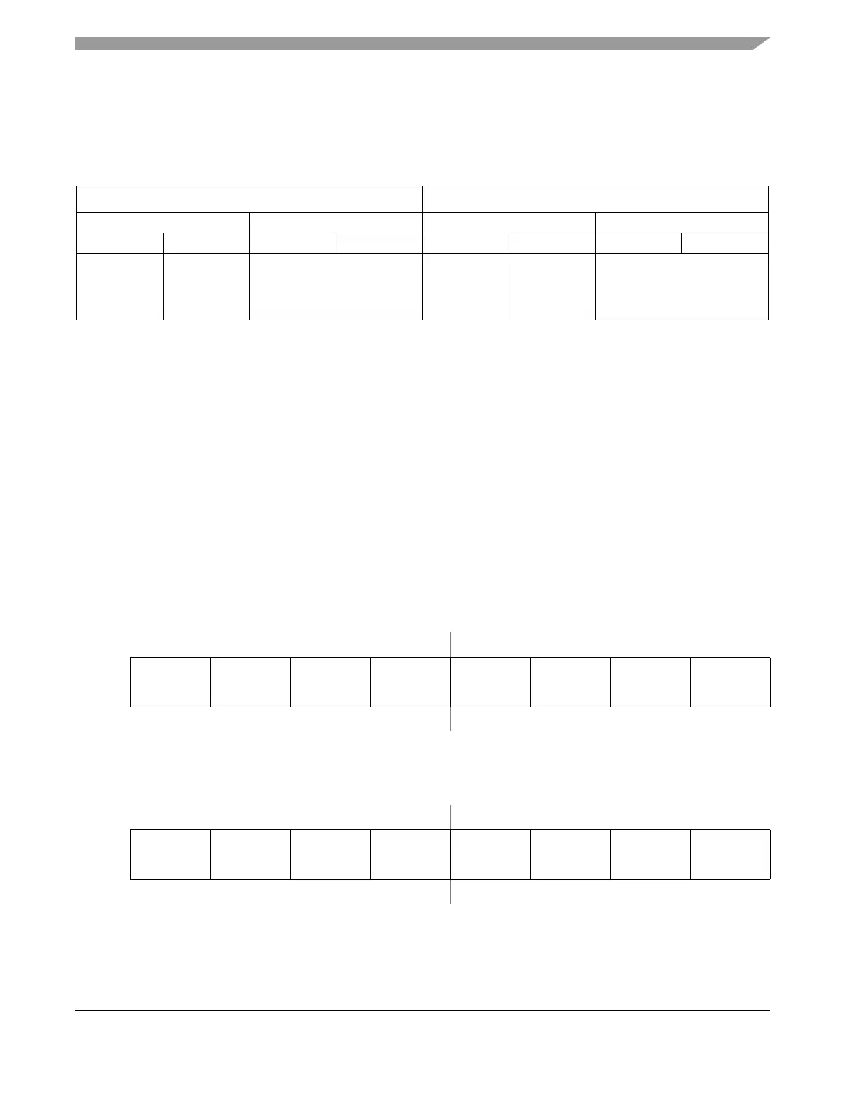
Table 23-10. The OC7 and OCx event priority
OC7M7=0 OC7M7=1
OC7Mx=1 OC7Mx=0 OC7Mx=1 OC7Mx=0
TC7=TCx TC7>TCx TC7=TCx TC7>TCx TC7=TCx TC7>TCx TC7=TCx TC7>TCx
IOCx=OC7Dx
IOC7=OM7/O
L7
IOCx=OC7Dx
+OMx/OLx
IOC7=OM7/O
L7
IOCx=OMx/OLx
IOC7=OM7/OL7
IOCx=OC7Dx
IOC7=OC7D7
IOCx=OC7Dx
+OMx/OLx
IOC7=OC7D7
IOCx=OMx/OLx
IOC7=OC7D7
Module Base + 0x000A
76543210
R
EDG7B EDG7A EDG6B EDG6A EDG5B EDG5A EDG4B EDG4A
W
Reset00000000
Figure 23-16. Timer Control Register 3 (TCTL3)
Module Base + 0x000B
76543210
R
EDG3B EDG3A EDG2B EDG2A EDG1B EDG1A EDG0B EDG0A
W
Reset00000000
Figure 23-17. Timer Control Register 4 (TCTL4)

 Loading...


