32 KByte Flash Module (S12FTMRG32K1V1)
MC9S12G Family Reference Manual Rev.1.27
822 NXP Semiconductors
25.3.2.1 Flash Clock Divider Register (FCLKDIV)
The FCLKDIV register is used to control timed events in program and erase algorithms.
All bits in the FCLKDIV register are readable, bit 7 is not writable, bit 6 is write-once-hi and controls the
writability of the FDIV field in normal mode. In special mode, bits 6-0 are writable any number of times
but bit 7 remains unwritable.
0x000D
FRSV2
R00000000
W
0x000E
FRSV3
R00000000
W
0x000F
FRSV4
R00000000
W
0x0010
FOPT
R NV7 NV6 NV5 NV4 NV3 NV2 NV1 NV0
W
0x0011
FRSV5
R00000000
W
0x0012
FRSV6
R00000000
W
0x0013
FRSV7
R00000000
W
= Unimplemented or Reserved
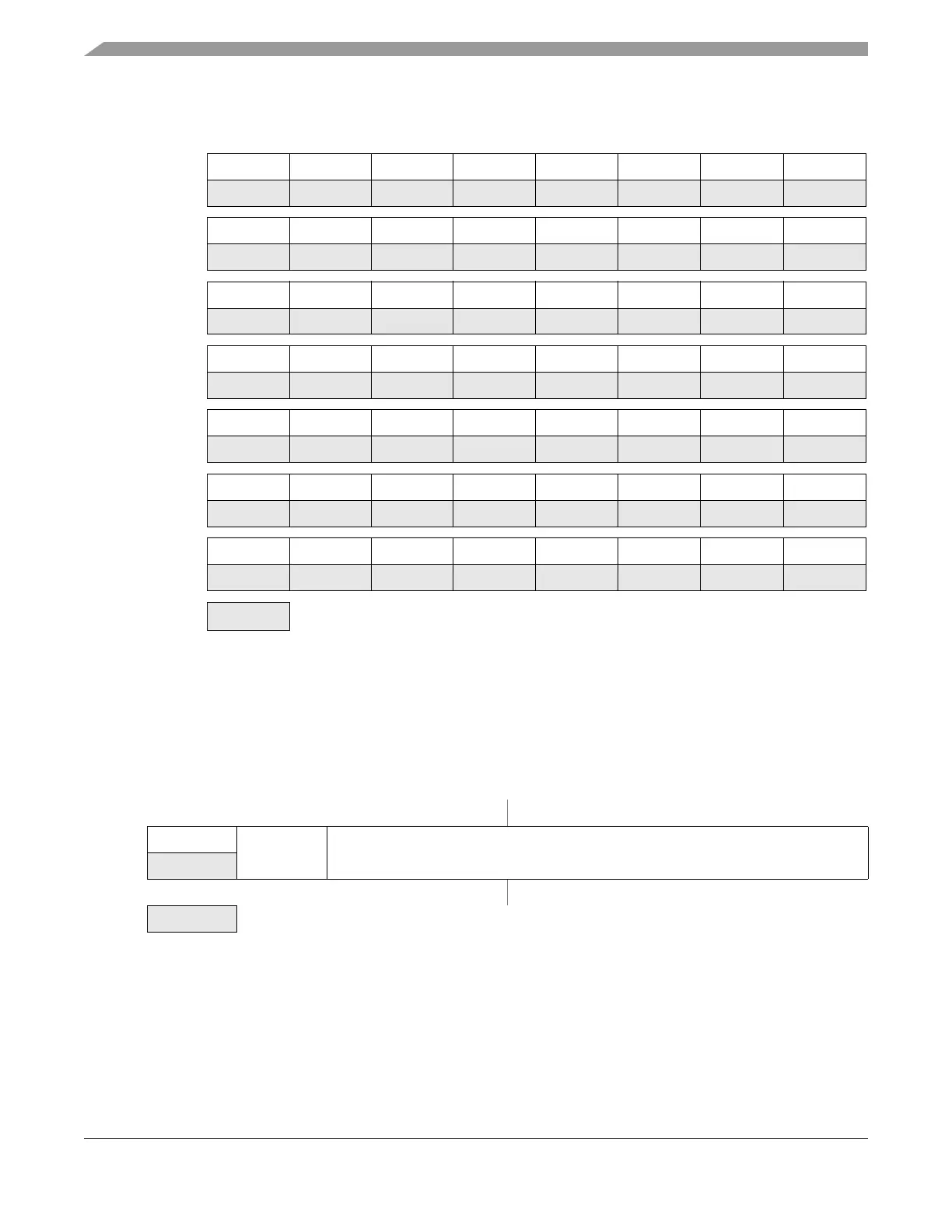
Offset Module Base + 0x0000
76543210
RFDIVLD
FDIVLCK FDIV[5:0]
W
Reset00000000
= Unimplemented or Reserved
Figure 25-5. Flash Clock Divider Register (FCLKDIV)
Address
& Name
76543210
Figure 25-4. FTMRG32K1 Register Summary (continued)

 Loading...


