32 KByte Flash Module (S12FTMRG32K1V1)
MC9S12G Family Reference Manual Rev.1.27
NXP Semiconductors 823
CAUTION
The FCLKDIV register should never be written while a Flash command is
executing (CCIF=0).
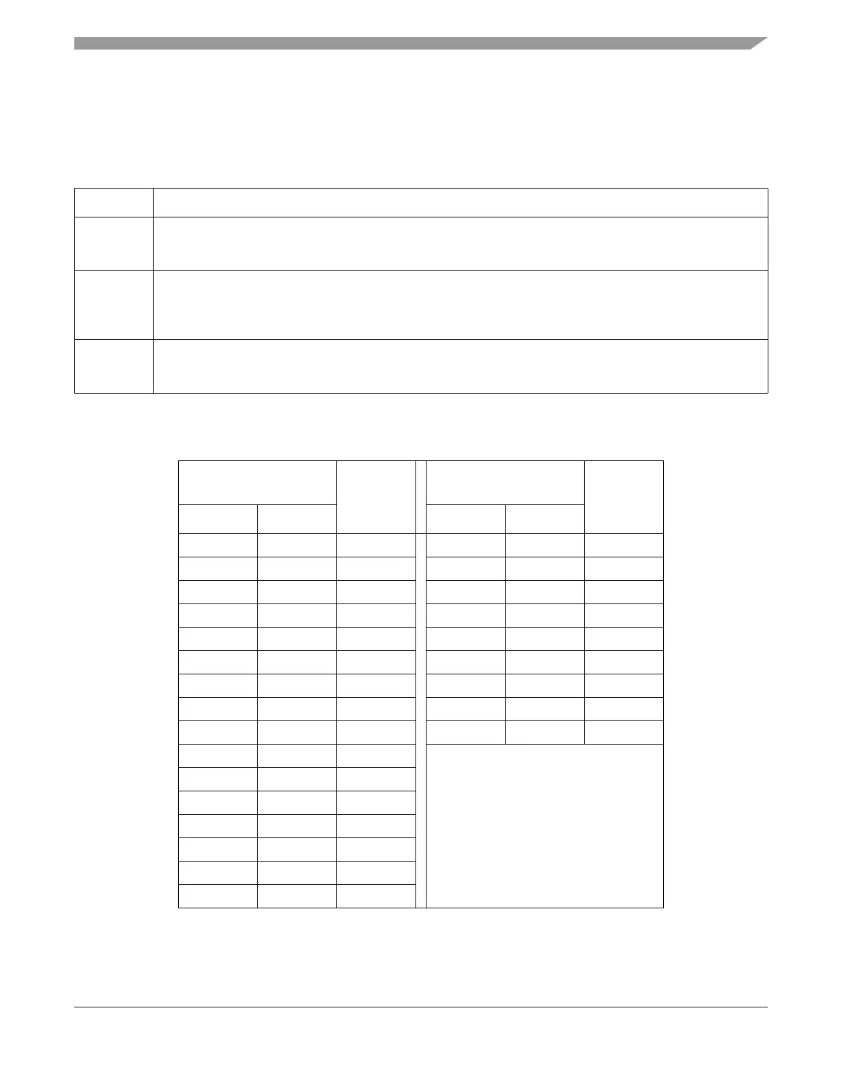
Table 25-7. FCLKDIV Field Descriptions
Field Description
7
FDIVLD
Clock Divider Loaded
0 FCLKDIV register has not been written since the last reset
1 FCLKDIV register has been written since the last reset
6
FDIVLCK
Clock Divider Locked
0 FDIV field is open for writing
1 FDIV value is locked and cannot be changed. Once the lock bit is set high, only reset can clear this bit and
restore writability to the FDIV field in normal mode.
5–0
FDIV[5:0]
Clock Divider Bits — FDIV[5:0] must be set to effectively divide BUSCLK down to 1 MHz to control timed events
during Flash program and erase algorithms. Table 25-8 shows recommended values for FDIV[5:0] based on the
BUSCLK frequency. Please refer to Section 25.4.4, “Flash Command Operations,” for more information.
Table 25-8. FDIV values for various BUSCLK Frequencies
BUSCLK Frequency
(MHz)
FDIV[5:0]
BUSCLK Frequency
(MHz)
FDIV[5:0]
MIN
1
1
BUSCLK is Greater Than this value.
MAX
2
2
BUSCLK is Less Than or Equal to this value.
MIN
1
MAX
2
1.0 1.6 0x00 16.6 17.6 0x10
1.6 2.6 0x01 17.6 18.6 0x11
2.6 3.6 0x02 18.6 19.6 0x12
3.6 4.6 0x03 19.6 20.6 0x13
4.6 5.6 0x04 20.6 21.6 0x14
5.6 6.6 0x05 21.6 22.6 0x15
6.6 7.6 0x06 22.6 23.6 0x16
7.6 8.6 0x07 23.6 24.6 0x17
8.6 9.6 0x08 24.6 25.6 0x18
9.6 10.6 0x09
10.6 11.6 0x0A
11.6 12.6 0x0B
12.6 13.6 0x0C
13.6 14.6 0x0D
14.6 15.6 0x0E
15.6 16.6 0x0F

 Loading...


