64 KByte Flash Module (S12FTMRG64K1V1)
MC9S12G Family Reference Manual Rev.1.27
928 NXP Semiconductors
27.3.2.2 Flash Security Register (FSEC)
The FSEC register holds all bits associated with the security of the MCU and Flash module.
All bits in the FSEC register are readable but not writable.
During the reset sequence, the FSEC register is loaded with the contents of the Flash security byte in the
Flash configuration field at global address 0x3_FF0F located in P-Flash memory (see Table 27-4) as
indicated by reset condition F in Figure 27-6. If a double bit fault is detected while reading the P-Flash
phrase containing the Flash security byte during the reset sequence, all bits in the FSEC register will be set
to leave the Flash module in a secured state with backdoor key access disabled.
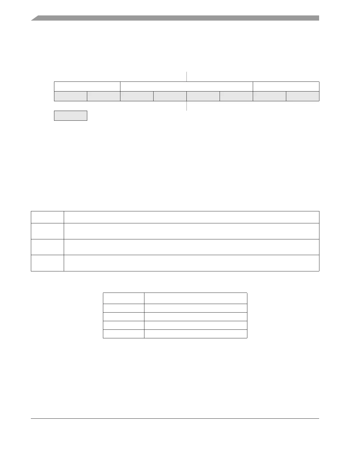
Offset Module Base + 0x0001
76543210
R KEYEN[1:0] RNV[5:2] SEC[1:0]
W
Reset F
1
1
Loaded from IFR Flash configuration field, during reset sequence.
F
1
F
1
F
1
F
1
F
1
F
1
F
1
= Unimplemented or Reserved
Figure 27-6. Flash Security Register (FSEC)
Table 27-9. FSEC Field Descriptions
Field Description
7–6
KEYEN[1:0]
Backdoor Key Security Enable Bits — The KEYEN[1:0] bits define the enabling of backdoor key access to the
Flash module as shown in Table 27-10.
5–2
RNV[5:2]
Reserved Nonvolatile Bits — The RNV bits should remain in the erased state for future enhancements.
1–0
SEC[1:0]
Flash Security Bits — The SEC[1:0] bits define the security state of the MCU as shown in Table 27-11. If the
Flash module is unsecured using backdoor key access, the SEC bits are forced to 10.
Table 27-10. Flash KEYEN States
KEYEN[1:0] Status of Backdoor Key Access
00 DISABLED
01 DISABLED
1
1
Preferred KEYEN state to disable backdoor key access.
10 ENABLED
11 DISABLED

 Loading...


