64 KByte Flash Module (S12FTMRG64K1V1)
MC9S12G Family Reference Manual Rev.1.27
938 NXP Semiconductors
During the reset sequence, fields DPOPEN and DPS of the EEPROT register are loaded with the contents
of the EEPROM protection byte in the Flash configuration field at global address 0x3_FF0D located in
P-Flash memory (see Table 27-4) as indicated by reset condition F in Table 27-23. To change the
EEPROM protection that will be loaded during the reset sequence, the P-Flash sector containing the
EEPROM protection byte must be unprotected, then the EEPROM protection byte must be programmed.
If a double bit fault is detected while reading the P-Flash phrase containing the EEPROM protection byte
during the reset sequence, the DPOPEN bit will be cleared and DPS bits will be set to leave the EEPROM
memory fully protected.
Trying to alter data in any protected area in the EEPROM memory will result in a protection violation error
and the FPVIOL bit will be set in the FSTAT register. Block erase of the EEPROM memory is not possible
if any of the EEPROM sectors are protected.
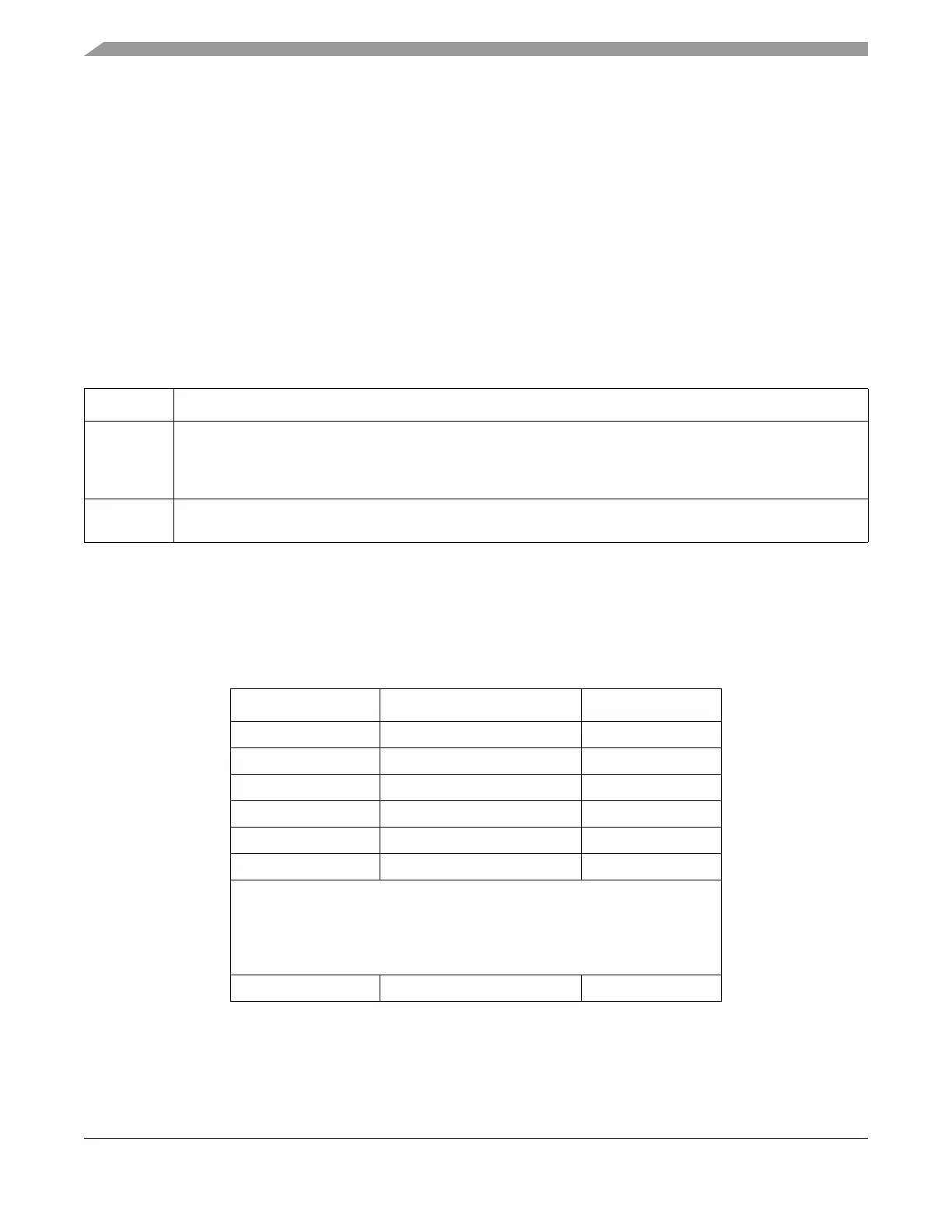
Table 27-22. EEPROT Field Descriptions
Field Description
7
DPOPEN
EEPROM Protection Control
0 Enables EEPROM memory protection from program and erase with protected address range defined by DPS
bits
1 Disables EEPROM memory protection from program and erase
5–0
DPS[5:0]
EEPROM Protection Size — The DPS[5:0] bits determine the size of the protected area in the EEPROM
memory as shown in Table 27-23 .
Table 27-23. EEPROM Protection Address Range
DPS[5:0] Global Address Range Protected Size
000000 0x0_0400 – 0x0_041F 32 bytes
000001 0x0_0400 – 0x0_043F 64 bytes
000010 0x0_0400 – 0x0_045F 96 bytes
000011 0x0_0400 – 0x0_047F 128 bytes
000100 0x0_0400 – 0x0_049F 160 bytes
000101 0x0_0400 – 0x0_04BF 192 bytes
The Protection Size goes on enlarging in step of 32 bytes, for each DPS value
increasing of one.
.
.
.
111111 0x0_0400 – 0x0_0BFF 2,048 bytes

 Loading...


