RL78/G15 CHAPTER 6 TIMER ARRAY UNIT
R01UH0959EJ0110 Rev.1.10 Page 171 of 765
Mar 7, 2023
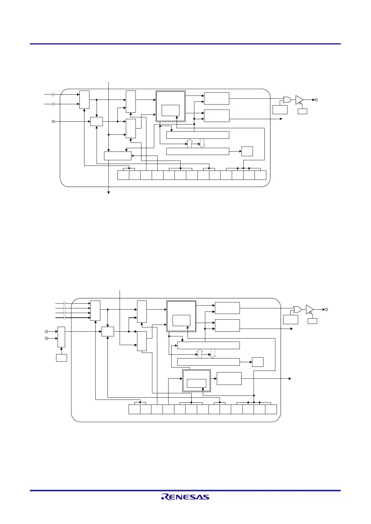
Figure 6-2. Internal Block Diagram of Channels 0, 2, 4, 6 of Timer Array Unit
CKS
0n
1
Timer controller
Edge
detection
Mode
selection
Interrupt
controller
Output
controller
OVF
0
n
CK
00
CK
01
TI0n
f
MCK
Timer counter register 0
n
(
TCR
0
n)
Timer data register 0n (TDR0n)
Slave
/
master
controller
Output latch
(Pxx)
TO0n
INTTM0n
(Timer interrupt
)
f
TCLK
Input signal to the slave channel
Timer mode register
0
n (
TMR0
n)
Overflow
Timer status register
0n (TSR0n)
Input signal from the master channel
Note 1
Operation
clock
selection
Count clock
selection
Channel n
CKS
0
n0
CCS0
n
MAS
TER
0n
Note 2
STS0n2 STS0n1 STS0n0 CIS
0n
1
CIS0
n
0 MD
0n
3
MD0
n2
MD
0n
1 MD
0
n0
PMxx
Trigger
selection
Note 1. Channels 2, 4, and 6 only
Note 2. n = 2, 4, 6 only
Remark n = 0, 2, 4, 6
Figure 6-3. Internal Block Diagram of Channel 1 of Timer Array Unit
Timer controller
Mode
selection
f
MCK
Edge
detection
Output
controller
Output latch
(Pxx)
OVF
0n
CK00
CK01
Timer counter register 0n (TCR0n)
Timer data register 0n (TDR0n)
CK02
CK03
Interrupt
controller
INTTM0nH
(
Timer interrupt)
Input signal from the master channel
Overflow
Timer status register
0n (TSR0n)
INTTM0n
(Timer interrupt)
Channel n
Timer mode register 0n (TMR0n)
CKS0n1
CKS0n0
CCS0n
SPLIT
0n
STS0n2
STS0n1 STS0
n0
CIS0n1 CIS0n0
MD0n3 MD0n2
MD0n1
MD0
n0
Operation
clock
selection
Count clock
selection
TI0n
f
TCLK
Interrupt
controller
8-bit timer
controller
Mode
selection
TO0n
RxD0
ISC
Input switch
control
register
(ISC)
PMxx
Trigger
selection
Selector
Remark n = 1
 Loading...


