RL78/G15 CHAPTER 10 A/D CONVERTER
R01UH0959EJ0110 Rev.1.10 Page 325 of 765
Mar 7, 2023
Caution 2. When the internal reference voltage is selected as the target of conversion by the A/D converter,
the internal reference voltage cannot be used as the reference voltage of the comparator.
Caution 3. Only rewrite the FR1, FR0, and LV0 bits while in the conversion standby state (ADCS = 0, ADCE =
1) or conversion is stopped (ADCS = 0, ADCE = 0). Rewriting the values of the FR1, FR0, and LV0
bits, and ADCS bits by an 8-bit manipulation instruction at the same time is prohibited.
Caution 4. The above conversion time does not include clock frequency errors. Select the conversion time,
taking clock frequency errors into consideration.
Remark f
CLK
: CPU/peripheral hardware clock frequency
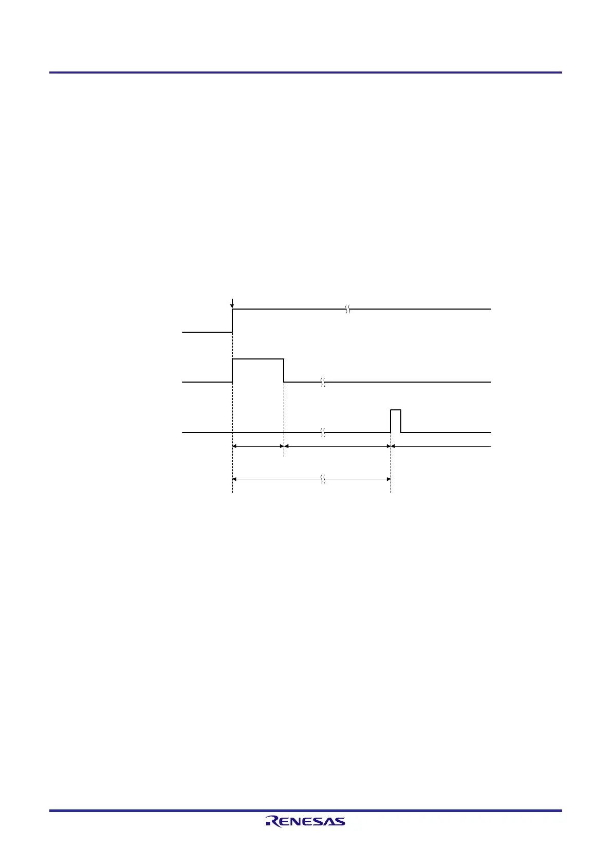
Figure 10-5. A/D Converter Sampling and A/D Conversion Timing
Conversion standby stateSampling
Sampling timing
ADCS ← 1
ADCS
Conversion time
INTAD
Successive conversion
 Loading...


