RL78/G15 CHAPTER 2 PIN FUNCTIONS
R01UH0959EJ0110 Rev.1.10 Page 54 of 765
Mar 7, 2023
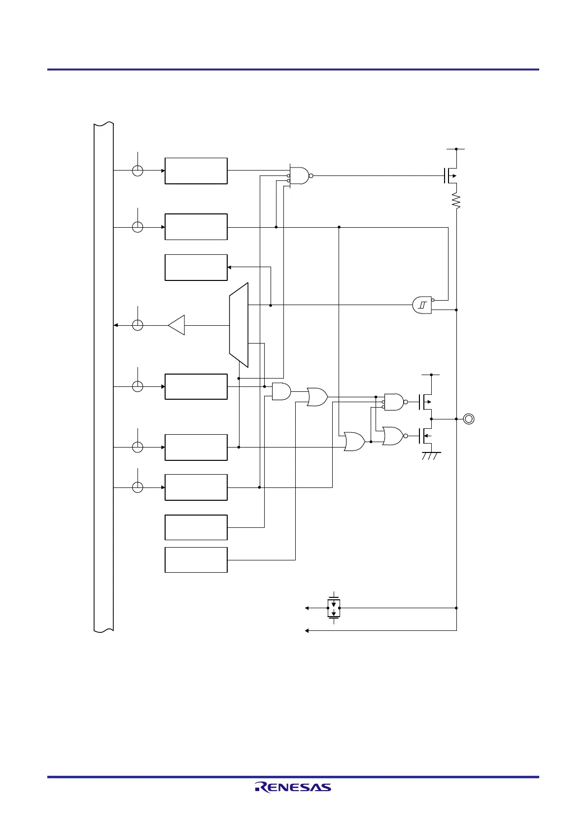
Figure 2-9. Pin Block Diagram for Pin Type 7-9-2
Output latch
(
Pmn)
WR
PU
Alternate function
Alternate function
(SAU)
Alternate function
(other than SAU)
PU register
(
PUmn)
Pmn
P-ch
P-ch
N
-ch
V
DD
V
DD
V
SS
1
0
RD
PORT
WR
PORT
PM register
(PMmn)
WR
PM
WR
PMC
PMC register
(PMCmn
)
P
-ch
N-ch
A/D converter
POM register
(POMmn)
WR
POM
Comparator input
Internal bus
Caution The input buffer is enabled even if the type 7-9-2 pin is operating as an output when the N-ch open
drain output mode is selected by the corresponding bit in the port output mode register (POMxx).
This may lead to a through current flowing through the type 7-9-2 pin when the voltage level on this
pin is intermediate.
Remark 1. For alternate functions, see 2.1 Port Function.
Remark 2. SAU: Serial array unit
 Loading...


