RL78/G15 CHAPTER 19 FLASH MEMORY
R01UH0959EJ0110 Rev.1.10 Page 657 of 765
Mar 7, 2023
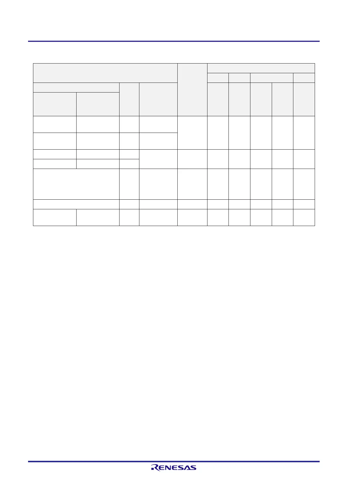
Table 19-2. Wiring between RL78/G15 and Dedicated Flash Memory Programmer
Pin Configuration of Dedicated Flash Memory Programmer Pin Name Pin No.
8-pin 10-pin 16-pin 20-pin
Signal Name I/O Pin Function WDFN SSOP SSOP HWQFN SSOP
PG-FP6
E2 or E2 Lite on-
chip debugging
emulator
— TOOL0 I/O
Transmit/
receive signal
TOOL0/P40 1 1 2 16 4
SI/RxD — I/O
Transmit/
receive signal
— RESET_OUT Output Reset signal RESET
¯¯¯¯¯¯
2 2 3 1 5
RESET
¯¯¯¯¯¯
— Output
V
DD
Note 1
I/O
V
DD
voltage
generation/
power
monitoring
V
DD
4 5 8 6 10
GND — Ground V
SS
3 4 7 5 9
FLMD1 EMV
DD
—
Driving power
for TOOL0 pin
V
DD
4 5 8 6 10
Note 1. The signal name for the PG-FP6 is V
CC
.
Remark Pins that are not indicated in the above table can be left open when using the flash memory programmer for
flash programming.
About a connection between RL78 microcontroller and a connector, refer to the user’s manual of each programmer.
About a connection with E2 or E2 Lite, see 20.1 Connecting E2, E2 Lite On-chip Debugging Emulator.
 Loading...


