RL78/G15 CHAPTER 24 ELECTRICAL SPECIFICATIONS (T
A
= −40 to +105°C, TA = −40 to +125°C)
R01UH0959EJ0110 Rev.1.10 Page 742 of 765
Mar 7, 2023
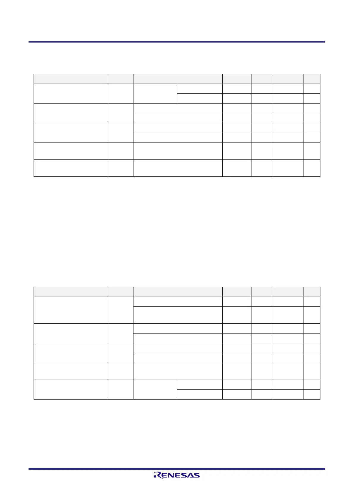
(2) Simplified SPI (CSI) mode (master mode, SCKp... internal clock output)
[T
A
= −40 to +105°C: G products, T
A
= −40 to +125°C: M products, 2.4 V ≤ V
DD
≤ 5.5 V, V
SS
= 0 V]
Item Symbol Condition MIN. TYP. MAX. Unit
SCKp cycle time t
KCY1
t
KCY1
≥ 4/f
CLK
2.7 V ≤ V
DD
≤ 5.5 V 250 ns
2.4 V ≤ V
DD
≤ 5.5 V 500 ns
SCKp high-/low-level width t
KH1
, t
KL1
2.7 V ≤ V
DD
≤ 5.5 V
t
KCY1
/2 − 36 ns
2.4 V ≤ V
DD
≤ 5.5 V
t
KCY1
/2 − 76 ns
SIp setup time
(to SCKp ↑)
Note 1
t
SIK1
2.7 V ≤ V
DD
≤ 5.5 V
66 ns
2.4 V ≤ V
DD
≤ 5.5 V
113 ns
SIp hold time
(from SCKp ↑)
Note 1
t
KSI1
38 ns
Delay time from SCKp ↓ to SOp
output
Note 2
t
KSO1
C = 30 pF
Note 3
66 ns
Note 1. When DAP0n = 0 and CKP0n = 0, or DAP0n = 1 and CKP0n = 1. The SIp setup time becomes “to SCKp ↓”
and the SIp hold time becomes “from SCKp ↓” when DAP0n = 0 and CKP0n = 1, or DAP0n = 1 and CKP0n =
0.
Note 2. When DAP0n = 0 and CKP0n = 0, or DAP0n = 1 and CKP0n = 1. The delay time to SOp output becomes
“from SCKp ↓” when DAP0n = 0 and CKP0n = 1, or DAP0n = 1 and CKP0n = 0.
Note 3. C is the load capacitance of the SCKp and SOp output lines.
(3) Simplified SPI (CSI) mode (slave mode, SCKp... external clock input)
[T
A
= −40 to +105°C: G products, T
A
= −40 to +125°C: M products, 2.4 V ≤ V
DD
≤ 5.5 V, V
SS
= 0 V]
Item Symbol Condition MIN. TYP. MAX. Unit
SCKp cycle time t
KCY2
2.7 V ≤ V
DD
≤ 5.5 V
12/f
MCK
ns
2.4 V ≤ V
DD
≤ 5.5 V
12/f
MCK
and
also 1000
ns
SCKp high-/low-level width t
KH2
,t
KL2
2.7 V ≤ V
DD
≤ 5.5 V
t
KCY2
/2 − 16 ns
2.4 V ≤ V
DD
≤ 5.5 V
t
KCY2
/2 − 36 ns
SIp setup time
(to SCKp ↑)
Note 1
t
SIK2
2.7 V ≤ V
DD
≤ 5.5 V
1/f
MCK
+ 40 ns
2.4 V ≤ V
DD
≤ 5.5 V
1/f
MCK
+ 60 ns
SIp hold time
(from SCKp ↑)
Note 1
t
KSI2
2.4 V ≤ V
DD
≤ 5.5 V
1/f
MCK
+ 62 ns
Delay time from SCKp ↓ to SOp
output
Note 2
t
KSO2
C = 30 pF
Note 3
2.7 V ≤ V
DD
≤ 5.5 V 2/f
MCK
+ 66 ns
2.4V ≤ V
DD
≤ 5.5V 2/f
MCK
+ 113 ns
Note 1. When DAP0n = 0 and CKP0n = 0, or DAP0n = 1 and CKP0n = 1. The SIp setup time becomes “to SCKp ↓”
and the SIp hold time becomes “from SCKp ↓” when DAP0n = 0 and CKP0n = 1, or DAP0n = 1 and CKP0n =
0.
Note 2. When DAP0n = 0 and CKP0n = 0, or DAP0n = 1 and CKP0n = 1. The delay time to SOp output becomes
“from SCKp ↓” when DAP0n = 0 and CKP0n = 1, or DAP0n = 1 and CKP0n = 0.
Note 3. C is the load capacitance of the SOp output lines.
 Loading...


