7–8 Chapter 7: External Memory Interfaces in Cyclone IV Devices
Cyclone IV Devices Memory Interfaces Pin Support
Cyclone IV Device Handbook, March 2016 Altera Corporation
Volume 1
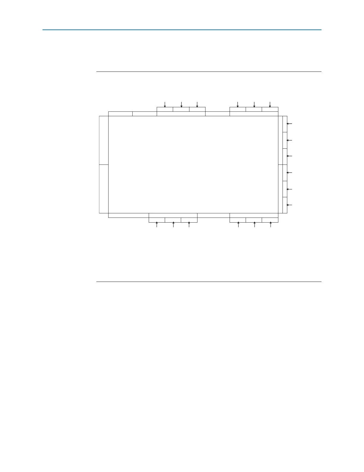
Figure 7–2 shows the location and numbering of the
DQS
,
DQ
, or CQ# pins in the
Cyclone IV GX I/O banks.
Figure 7–2. DQS, CQ, or CQ# Pins in Cyclone IV GX I/O Banks
(1)
Note to Figure 7–2:
(1) The DQS, CQ, or CQ# pin locations in this diagram apply to all packages in Cyclone IV GX devices except devices in
169-pin FBGA and 324-pin FBGA.
I/O Bank 8B
I/O Bank 3B I/O Bank 3 I/O Bank 3A I/O Bank 4
I/O Bank 8 I/O Bank 8A I/O Bank 7I/O Bank 9
Transceiver Block (QL1)Transceiver Block (QL0)
I/O Bank 6
I/O Bank 5
Cyclone IV GX Device
DQS4T/CQ5T
DQS2T/CQ3T
DQS0T/CQ1T
DQS4R/CQ5R
DQS2R/CQ3R
DQS0R/CQ1R
DQS1R/CQ1R#
DQS3R/CQ3R#
DQS5R/CQ5R#
DQS1B/CQ1B#
DQS3B/CQ3B#
DQS5B/CQ5B#
DQS4B/CQ5B
DQS2B/CQ3B
DQS0B/CQ1B
DQS1T/CQ1T#
DQS3T/CQ3T#
DQS5T/CQ5T#