Package and Die Information
MC9S12G Family Reference Manual Rev.1.27
NXP Semiconductors 1275
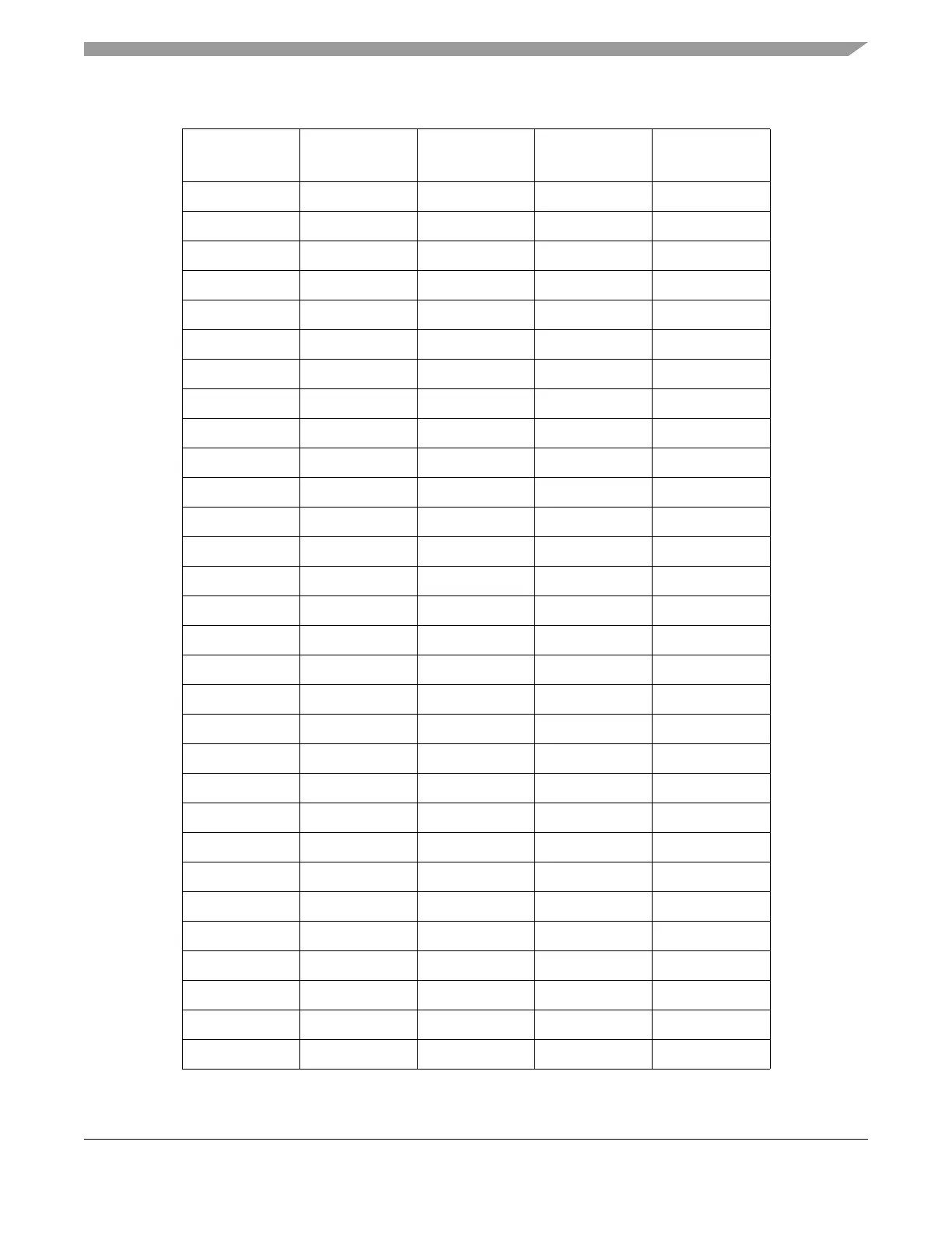
58 58 -1832.06 -467.5 PAD[9]
59 59 -1832.06 -360.5 PAD[2]
60 60 -1832.06 -253.5 PAD[10]
61 61 -1832.06 -148.5 PAD[3]
62 62 -1832.06 -41.5 PAD[11]
63 63 -1832.06 65.5 PAD[4]
64 64 -1832.06 172.5 PAD[12]
65 65 -1832.06 279.5 PAD[5]
66 66 -1832.06 386.5 PAD[13]
67 67 -1832.06 493.5 PAD[6]
68 68 -1832.06 598.5 PAD[14]
69 69 -1832.06 705.5 PAD[7]
70 70 -1832.06 812.5 PAD[15]
71 71 -1832.06 919.5 PC[4]
72 72 -1832.06 1026.5 PC[5]
73 73 -1832.06 1133.5 PC[6]
74 74 -1832.06 1240.5 PC[7]
75 75 -1832.06 1347.5 VRH
76 76 1707.5 -1472.06 VDDA
77 77 1598.5 -1472.06 VRL
78 77 1477.5 -1472.06 VSSA
79 78 1237.5 -1472.06 PD[0]
80 79 1117.5 -1472.06 PD[1]
81 80 947.5 -1472.06 PD[2]
82 81 777.5 -1472.06 PD[3]
83 82 652.5 -1472.06 PS[0]
84 83 527.5 -1472.06 PS[1]
85 84 422.5 -1472.06 PS[2]
86 85 327.5 -1472.06 PS[3]
87 86 242.5 -1472.06 PS[4]
Table D-1. Bondpad Coordinates
Die Pad Bond Post
Die Pad
X Coordinate
Die Pad
Y Coordinate
Function

 Loading...


