S12 Clock, Reset and Power Management Unit (S12CPMU)
MC9S12G Family Reference Manual Rev.1.27
370 NXP Semiconductors
Table 10-6. COPOSCSEL1, COPOSCSEL0 clock source select description
10.3.2.7 S12CPMU PLL Control Register (CPMUPLL)
This register controls the PLL functionality.
Read: Anytime
Write: Anytime if PROT=0 (CPMUPROT register) and PLLSEL=1 (CPMUCLKS register). Else write
has no effect.
NOTE
Write to this register clears the LOCK and UPOSC status bits.
1
RTIOSCSEL
RTI Clock Select — RTIOSCSEL selects the clock source to the RTI. Either IRCCLK or OSCCLK. Changing the
RTIOSCSEL bit re-starts the RTI time-out period.
RTIOSCSEL can only be set to 1, if UPOSC=1.
UPOSC= 0 clears the RTIOSCSEL bit.
0 RTI clock source is IRCCLK.
1 RTI clock source is OSCCLK.
0
COP
OSCSEL0
COP Clock Select 0 — COPOSCSEL0 and COPOSCSEL1 combined determine the clock source to the COP
(see also Table 10-6)
If COPOSCSEL1 = 1, COPOSCSEL0 has no effect regarding clock select and changing the COPOSCSEL0 bit
does not re-start the COP time-out period.
When COPOSCSEL1=0,COPOSCSEL0 selects the clock source to the COP to be either IRCCLK or OSCCLK.
Changing the COPOSCSEL0 bit re-starts the COP time-out period.
COPOSCSEL0 can only be set to 1, if UPOSC=1.
UPOSC= 0 clears the COPOSCSEL0 bit.
0 COP clock source is IRCCLK.
1 COP clock source is OSCCLK
COPOSCSEL1 COPOSCSEL0 COP clock source
00IRCCLK
01OSCCLK
1xACLK
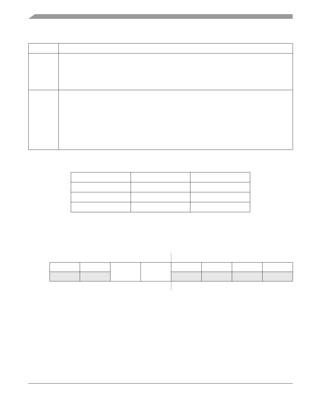
0x003A
76543210
R0 0
FM1 FM0
0000
W
Reset00000000
Figure 10-10. S12CPMU PLL Control Register (CPMUPLL)
Table 10-5. CPMUCLKS Descriptions (continued)
Field Description

 Loading...


