S12 Clock, Reset and Power Management Unit (S12CPMU)
MC9S12G Family Reference Manual Rev.1.27
NXP Semiconductors 371
NOTE
Care should be taken to ensure that the bus frequency does not exceed the
specified maximum when frequency modulation is enabled.
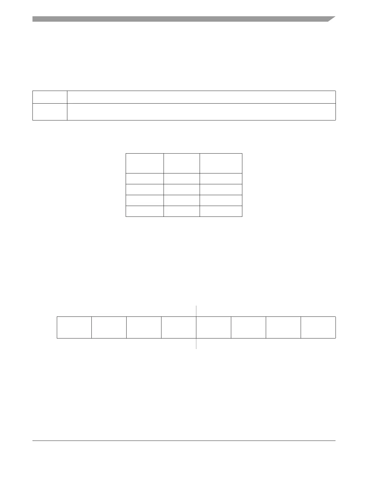
10.3.2.8 S12CPMU RTI Control Register (CPMURTI)
This register selects the time-out period for the Real Time Interrupt.
The clock source for the RTI is either IRCCLK or OSCCLK depending on the setting of the RTIOSCSEL
bit. In Stop Mode with PSTP=1 (Pseudo Stop Mode) and RTIOSCSEL=1 the RTI continues to run, else
the RTI counter halts in Stop Mode.
Read: Anytime
Write: Anytime
Table 10-7. CPMUPLL Field Descriptions
Field Description
5, 4
FM1, FM0
PLL Frequency Modulation Enable Bits — FM1 and FM0 enable frequency modulation on the VCOCLK. This
is to reduce noise emission. The modulation frequency is f
ref
divided by 16. See Table 10-8 for coding.
Table 10-8. FM Amplitude selection
FM1 FM0
FM Amplitude /
f
VCO
Variation
00 FM off
01 1%
10 2%
11 4%
0x003B
76543210
R
RTDEC RTR6 RTR5 RTR4 RTR3 RTR2 RTR1 RTR0
W
Reset00000000
Figure 10-11. S12CPMU RTI Control Register (CPMURTI)

 Loading...


