Timer Module (TIM16B8CV3)
MC9S12G Family Reference Manual Rev.1.27
752 NXP Semiconductors
NOTE
The newly selected prescale factor will not take effect until the next
synchronized edge where all prescale counter stages equal zero.
23.3.2.12 Main Timer Interrupt Flag 1 (TFLG1)
Read: Anytime
Write: Used in the clearing mechanism (set bits cause corresponding bits to be cleared). Writing a zero will
not affect current status of the bit.
23.3.2.13 Main Timer Interrupt Flag 2 (TFLG2)
TFLG2 indicates when interrupt conditions have occurred. To clear a bit in the flag register, write the bit
to one while TEN bit of TSCR1 or PAEN bit of PACTL is set to one.
Read: Anytime
Write: Used in clearing mechanism (set bits cause corresponding bits to be cleared).
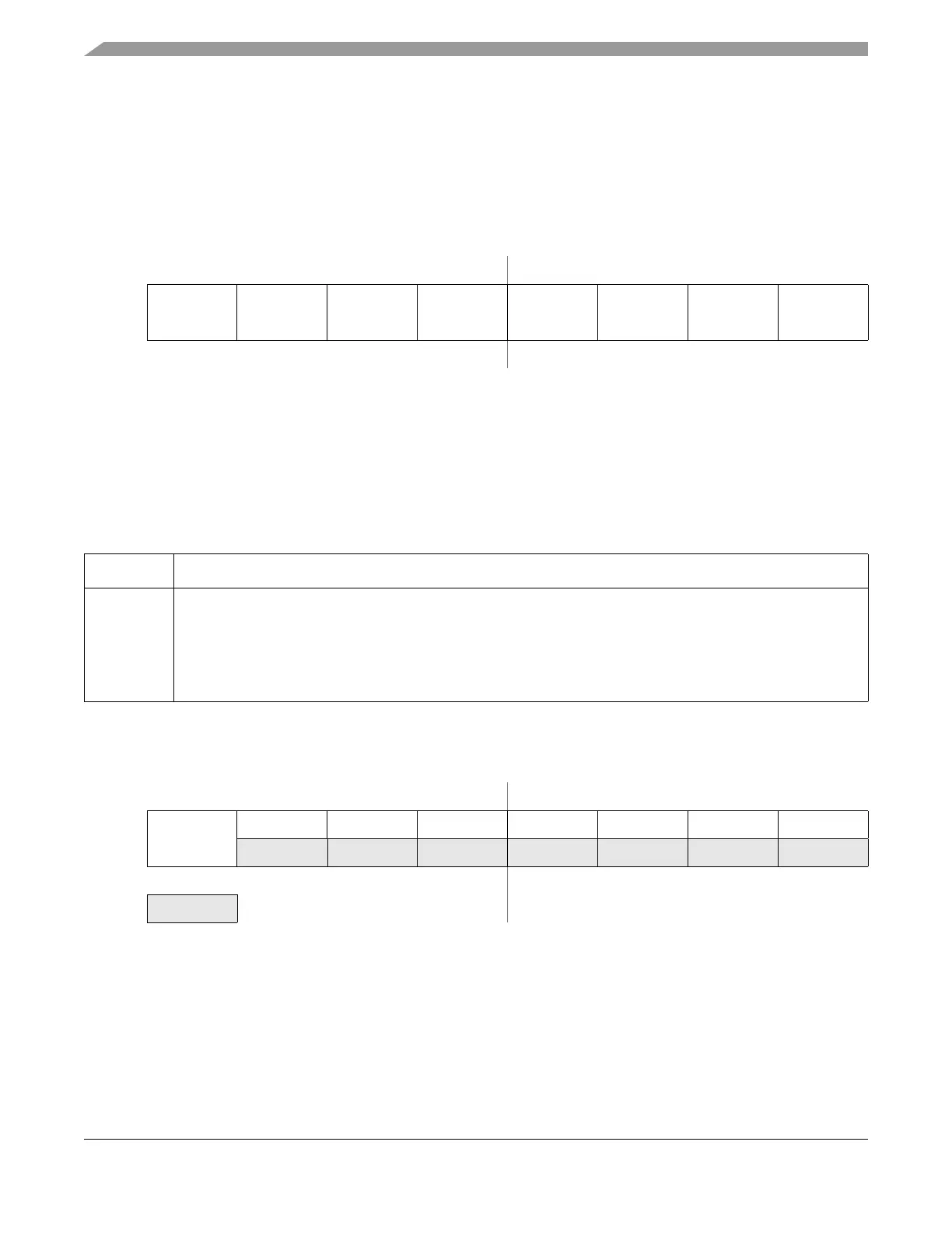
Module Base + 0x000E
76543210
R
C7F C6F C5F C4F C3F C2F C1F C0F
W
Reset00000000
Figure 23-20. Main Timer Interrupt Flag 1 (TFLG1)
Table 23-16. TRLG1 Field Descriptions
Note: Writing to unavailable bits has no effect. Reading from unavailable bits return a zero.
Field Description
7:0
C[7:0]F
Input Capture/Output Compare Channel “x” Flag — These flags are set when an input capture or output
compare event occurs. Clearing requires writing a one to the corresponding flag bit while TEN or PAEN is set to
one.
Note: When TFFCA bit in TSCR register is set, a read from an input capture or a write into an output compare
channel (0x0010–0x001F) will cause the corresponding channel flag CxF to be cleared.
Module Base + 0x000F
76543210
R
TOF
0000000
W
Reset00000000
Unimplemented or Reserved
Figure 23-21. Main Timer Interrupt Flag 2 (TFLG2)

 Loading...


