Timer Module (TIM16B8CV3)
MC9S12G Family Reference Manual Rev.1.27
NXP Semiconductors 753
Any access to TCNT will clear TFLG2 register if the TFFCA bit in TSCR register is set.
23.3.2.14 Timer Input Capture/Output Compare Registers High and Low 0–
7(TCxH and TCxL)
1
This register is available only when the corresponding channel exists and is reserved if that channel does not exist. Writes to
a reserved register have no functional effect. Reads from a reserved register return zeroes.
Depending on the TIOS bit for the corresponding channel, these registers are used to latch the value of the
free-running counter when a defined transition is sensed by the corresponding input capture edge detector
or to trigger an output action for output compare.
Read: Anytime
Write: Anytime for output compare function.Writes to these registers have no meaning or effect during
input capture. All timer input capture/output compare registers are reset to 0x0000.
NOTE
Read/Write access in byte mode for high byte should take place before low
byte otherwise it will give a different result.
Table 23-17. TRLG2 Field Descriptions
Field Description
7
TOF
Timer Overflow Flag — Set when 16-bit free-running timer overflows from 0xFFFF to 0x0000. Clearing this bit
requires writing a one to bit 7 of TFLG2 register while the TEN bit of TSCR1 or PAEN bit of PACTL is set to one
(See also TCRE control bit explanation) .
Module Base + 0x0010 = TC0H
0x0012 = TC1H
0x0014=TC2H
0x0016=TC3H
0x0018=TC4H
0x001A=TC5H
0x001C=TC6H
0x001E=TC7H
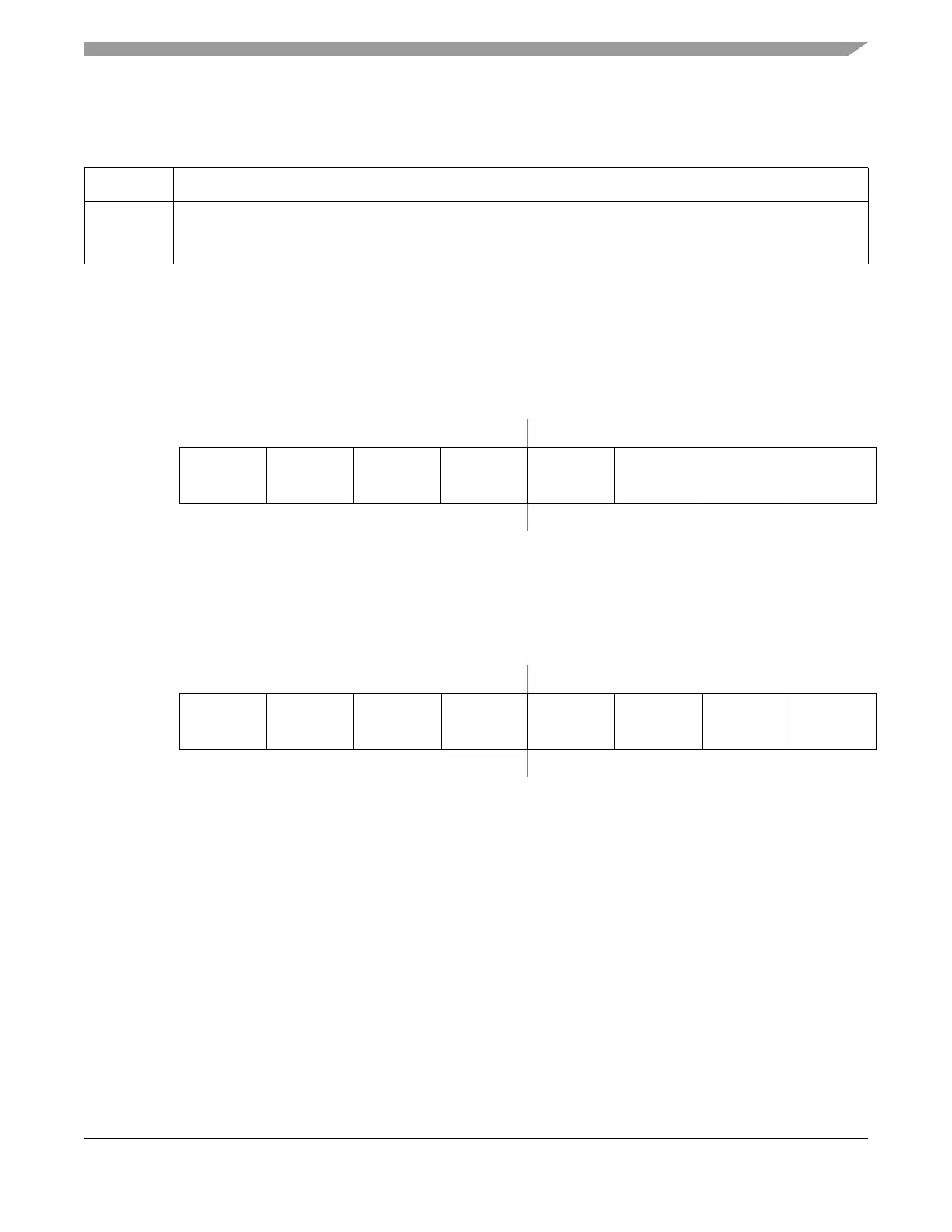
15 14 13 12 11 10 9 0
R
Bit 15 Bit 14 Bit 13 Bit 12 Bit 11 Bit 10 Bit 9 Bit 8
W
Reset00000000
Figure 23-22. Timer Input Capture/Output Compare Register x High (TCxH)
Module Base + 0x0011 = TC0L
0x0013 = TC1L
0x0015 =TC2L
0x0017=TC3L
0x0019 =TC4L
0x001B=TC5L
0x001D=TC6L
0x001F=TC7L
76543210
R
Bit 7Bit 6Bit 5Bit 4Bit 3Bit 2Bit 1Bit 0
W
Reset00000000
Figure 23-23. Timer Input Capture/Output Compare Register x Low (TCxL)

 Loading...


