Chapter 6: I/O Features in Cyclone IV Devices 6–21
I/O Banks
March 2016 Altera Corporation Cyclone IV Device Handbook,
Volume 1
Each Cyclone IV I/O bank has its own
VCCIO
pins. Each I/O bank can support only one V
CCIO
setting from among 1.2, 1.5, 1.8,
2.5, 3.0, or 3.3 V. Any number of supported single-ended or differential standards can be simultaneously supported in a single
I/O bank, as long as they use the same V
CCIO
levels for input and output pins.
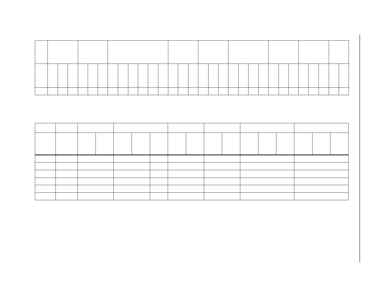
8 111111222222111444444422233333
Note to Table 6–4:
(1) User I/O pins are used as inputs or outputs; clock input pins are used as inputs only; clock output pins are used as output only.
Table 6–4. Number of VREF Pins Per I/O Bank for Cyclone IV E Devices (Part 2 of 2)
Device
EP4CE6
EP4CE10
EP4CE15
EP4CE22
EP4CE30
EP4CE40
EP4CE55
EP4CE75
EP4CE115
I/O
Bank
(1)
144-EQPF
256-UBGA
256-FBGA
144-EQPF
256-UBGA
256-FBGA
144-EQPF
164-MBGA
256-MBGA
256-UBGA
256-FBGA
484-FBGA
144-EQPF
256-UBGA
256-FBGA
324-FBGA
484-FBGA
780-FBGA
324-FBGA
484-UBGA
484-FBGA
780-FBGA
484-UBGA
484-FBGA
780-FBGA
484-UBGA
484-FBGA
780-FBGA
484-FBGA
780-FBGA
Table 6–5. Number of VREF Pins Per I/O Bank for Cyclone IV GX Devices
Device 4CGX15 4CGX22 4CGX30 4CGX50 4CGX75 4CGX110 4CGX150
I/O Bank
(1)
169-FBGA
169-FBGA
324-FBGA
169-FBGA
324-FBGA
484-FBGA
484-FBGA
672-FBGA
484-FBGA
672-FBGA
484-FBGA
672-FBGA
896-FBGA
484-FBGA
672-FBGA
896-FBGA
31 1 1 3 3 3 3 3
41 1 1 3 3 3 3 3
51 1 1 3 3 3 3 3
61 1 1 3 3 3 3 3
71 1 1 3 3 3 3 3
8
(2)
11 133 3 3 3
Notes to Table 6–5:
(1) User I/O pins are used as inputs or outputs; clock input pins are used as inputs only; clock output pins are used as output only.
(2) Bank 9 does not have
VREF
pin. If input pins with
VREF
I/O standards are used in bank 9 during user mode, it shares the
VREF
pin in bank 8.