Chapter 6: I/O Features in Cyclone IV Devices 6–25
High-Speed I/O Interface
March 2016 Altera Corporation Cyclone IV Device Handbook,
Volume 1
Tab le 6 –6 and Tab le 6– 7 summarize which I/O banks support these I/O standards in
the Cyclone IV device family.
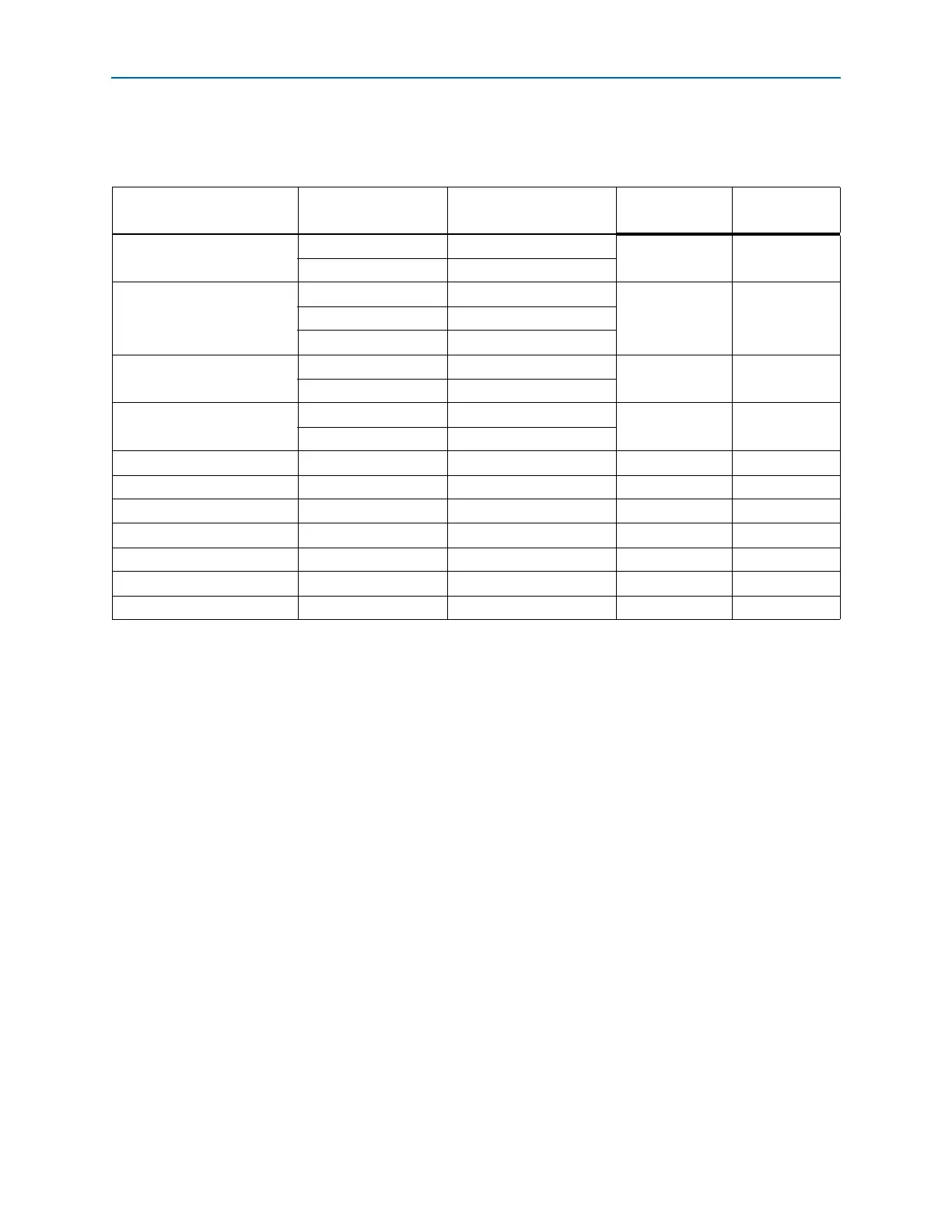
Table 6–6. Differential I/O Standards Supported in Cyclone IV E I/O Banks
Differential I/O Standards I/O Bank Location
External Resistor
Network at Transmitter
Transmitter (TX) Receiver (RX)
LVDS
1,2,5,6 Not Required
vv
All Three Resistors
RSDS
1,2,5,6 Not Required
v —3,4,7,8 Three Resistors
All Single Resistor
mini-LVDS
1,2,5,6 Not Required
v —
All Three Resistors
PPDS
1,2,5,6 Not Required
v —
All Three Resistors
BLVDS
(1)
All Single Resistor vv
LVPECL
(2)
All — — v
Differential SSTL-2
(3)
All — vv
Differential SSTL-18
(3)
All — vv
Differential HSTL-18
(3)
All — vv
Differential HSTL-15
(3)
All — vv
Differential HSTL-12
(3)
,
(4)
All — vv
Notes to Table 6–6:
(1) Transmitter and Receiver f
MAX
depend on system topology and performance requirement.
(2) The LVPECL I/O standard is only supported on dedicated clock input pins.
(3) The differential SSTL-2, SSTL-18, HSTL-18, HSTL-15, and HSTL-12 I/O standards are only supported on clock input pins and PLL output clock
pins. PLL output clock pins do not support Class II interface type of differential SSTL-18, HSTL-18, HSTL-15, and HSTL-12 I/O standards.
(4) Differential HSTL-12 Class II is supported only in column I/O banks.