8–20 Chapter 8: Configuration and Remote System Upgrades in Cyclone IV Devices
Configuration
Cyclone IV Device Handbook, May 2013 Altera Corporation
Volume 1
f For more information about the USB-Blaster download cable, refer to the USB-Blaster
Download Cable User Guide. For more information about the ByteBlaster II download
cable, refer to the ByteBlaster II Download Cable User Guide.
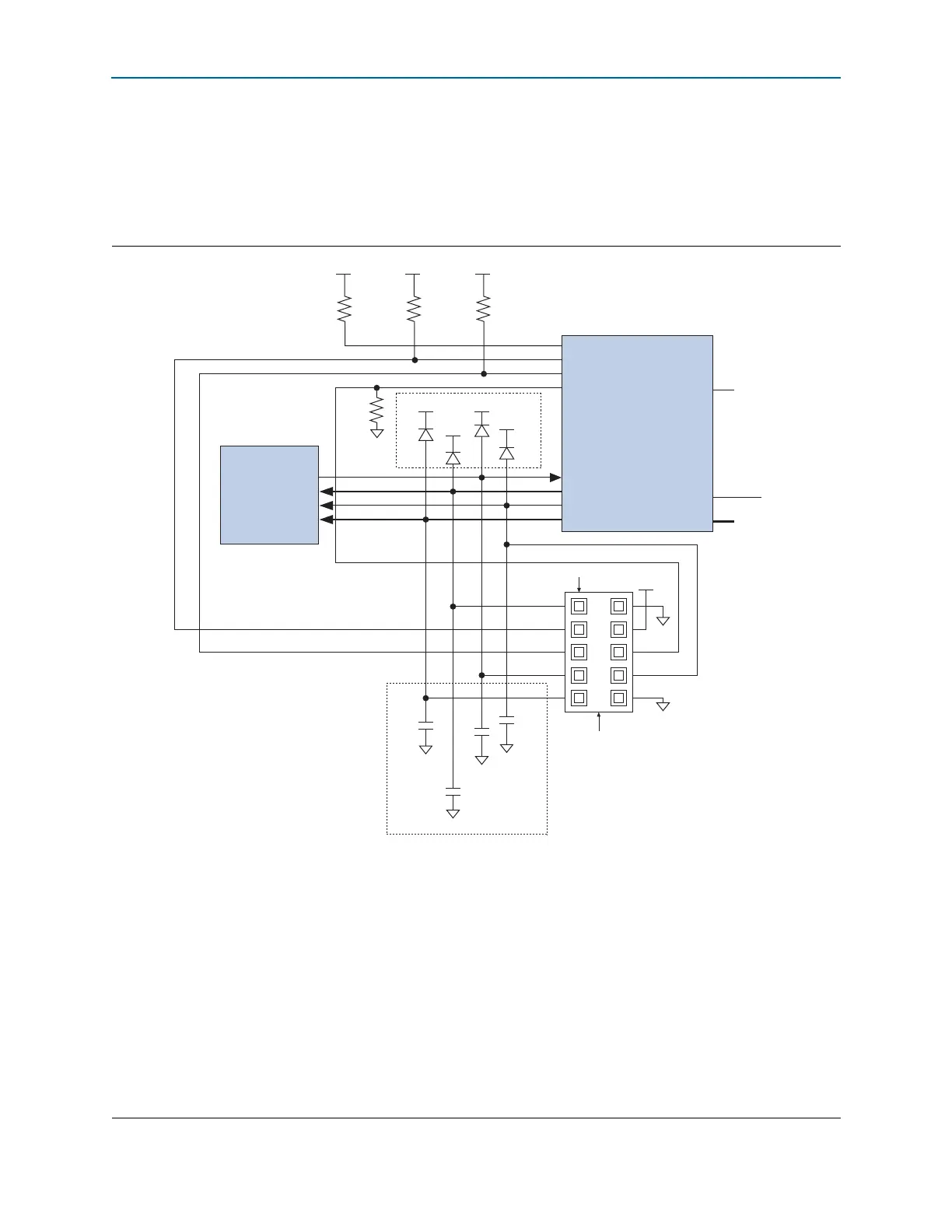
Figure 8–6 shows the download cable connections to the serial configuration device.
Figure 8–6. In-System Programming of Serial Configuration Devices
Notes to Figure 8–6:
(1) Connect these pull-up resistors to the V
CCIO
supply of the bank in which the pin resides.
(2) The
nCEO
pin is left unconnected or used as a user I/O pin when it does not feed the
nCE
pin of another device.
(3) Power up the V
CC
of the ByteBlaster II or USB-Blaster download cable with the 3.3-V supply.
(4) The
MSEL
pin settings vary for different configuration voltage standards and POR time. To connect the
MSEL
pins, refer to Table 8–3 on page 8–8,
Table 8–4 on page 8–8, and Table 8–5 on page 8–9. Connect the
MSEL
pins directly to V
CCA
or GND.
(5) The diodes and capacitors must be placed as close as possible to the Cyclone IV device. You must ensure that the diodes and capacitors maintain
a maximum AC voltage of 4.1 V. The external diodes and capacitors are required to prevent damage to the Cyclone IV device AS configuration
input pins due to possible overshoot when programming the serial configuration device with a download cable. Altera recommends using the
Schottky diode, which has a relatively lower forward diode voltage (VF) than the switching and Zener diodes, for effective voltage clamping.
(6) When cascading Cyclone IV devices in a multi-device AS configuration, connect the repeater buffers between the master and slave devices for
DATA[0]
and
DCLK
. All I/O inputs must maintain a maximum AC voltage of 4.1 V. The output resistance of the repeater buffers must fit the
maximum overshoot equation outlined in “Configuration and JTAG Pin I/O Requirements” on page 8–5.
(7) These pins are dual-purpose I/O pins. The
nCSO
pin functions as
FLASH_nCE
pin in AP mode. The
ASDO
pin functions as
DATA[1]
pin in AP and
FPP modes.
(8) Only Cyclone IV GX devices have an option to select CLKUSR (40 MHz maximum) as the external clock source for DCLK.
nSTATUS
nCONFIG
CONF_DONE
nCE
DATA[0] (6)
DCLK (6)
nCSO (7)
ASDO (7)
nCEO
MSEL[ ]
(4)
Cyclone IV Device
DATA
DCLK
nCS
ASDI
Serial
Configuration Device
GND
GND
N.C. (2)
V
CCIO
(1)
V
CCIO
(1)
V
CCIO
(1)
3.3 V
(3)
GND
Pin 1
ByteBlaster II or USB Blaster
10-Pin Male Header
3.3 V
10 pf
GND
GND
10 pf
(5)
10 pf
GND
10 pf
GND
(5)
10 k
Ω 10 kΩ 10 kΩ
10 kΩ
3.3 V
3.3 V
3.3 V
CLKUSR
(8)