8–48 Chapter 8: Configuration and Remote System Upgrades in Cyclone IV Devices
Configuration
Cyclone IV Device Handbook, May 2013 Altera Corporation
Volume 1
To configure a single device in a JTAG chain, the programming software places all
other devices in bypass mode. In bypass mode, devices pass programming data from
the
TDI
pin to the
TDO
pin through a single bypass register without being affected
internally. This scheme enables the programming software to program or verify the
target device. Configuration data driven into the device appears on the
TDO
pin one
clock cycle later.
The Quartus II software verifies successful JTAG configuration after completion. At
the end of configuration, the software checks the state of
CONF_DONE
through the JTAG
port. When Quartus II generates a .jam for a multi-device chain, it contains
instructions so that all the devices in the chain are initialized at the same time. If
CONF_DONE
is not high, the Quartus II software indicates that configuration has failed.
If
CONF_DONE
is high, the software indicates that configuration was successful. After
the configuration bitstream is serially sent using the JTAG
TDI
port, the
TCK
port
clocks an additional clock cycles to perform device initialization.
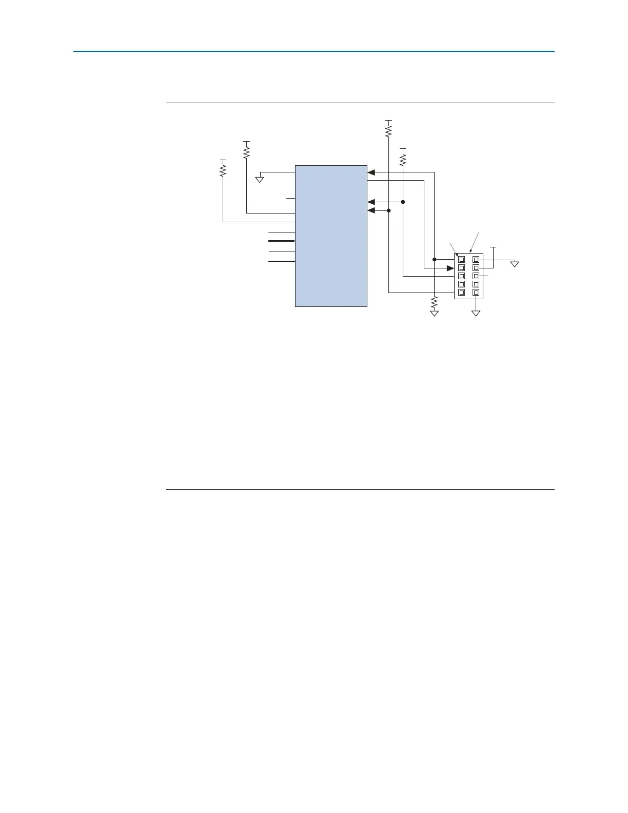
Figure 8–24. JTAG Configuration of a Single Device Using a Download Cable (1.5-V or 1.8-V V
CCIO
Powering the JTAG Pins)
Notes to Figure 8–24:
(1) Connect these pull-up resistors to the V
CCIO
supply of the bank in which the pin resides.
(2) Connect the
nCONFIG
and
MSEL
pins to support a non-JTAG configuration scheme. If you only use JTAG
configuration, connect the
nCONFIG
pin to logic-high and the
MSEL
pins to GND. In addition, pull
DCLK
and
DATA[0]
to either high or low, whichever is convenient on your board.
(3) In the USB-Blaster and ByteBlaster II cables, this pin is connected to
nCE
when it is used for AS programming;
otherwise it is a no connect.
(4) The
nCE
must be connected to GND or driven low for successful JTAG configuration.
(5) The
nCEO
pin is left unconnected or used as a user I/O pin when it does not feed the
nCE
pin of another device.
(6) Power up the V
CC
of the EthernetBlaster, ByteBlaster II or USB-Blaster cable with supply from V
CCIO
. The
Ethernet-Blaster, ByteBlaster II, and USB-Blaster cables do not support a target supply voltage of 1.2 V. For the target
supply voltage value, refer to the ByteBlaster II Download Cable User Guide, the USB-Blaster Download Cable User
Guide, and the EthernetBlaster Communications Cable User Guide.
(7) Resistor value can vary from 1 k to 10 k.
nCE (4)
MSEL[ ]
nCONFIG
CONF_DONE
V
CCIO
V
CCIO
(6)
GND
V
CCIO
(1)
GND
V
CCIO
(1)
(2)
V
CCIO
10 kΩ
10 kΩ
(7)
(7)
nSTATUS
Pin 1
Download Cable 10-Pin Male
Header (Top View)
GND
TCK
TDO
TMS
TDI
GND
V
IO
(3)
Cyclone IV Device
nCEO
N.C. (5)
DCLK
DATA[0]
(2)
(2)
(2)
1 kΩ