8–54 Chapter 8: Configuration and Remote System Upgrades in Cyclone IV Devices
Configuration
Cyclone IV Device Handbook, May 2013 Altera Corporation
Volume 1
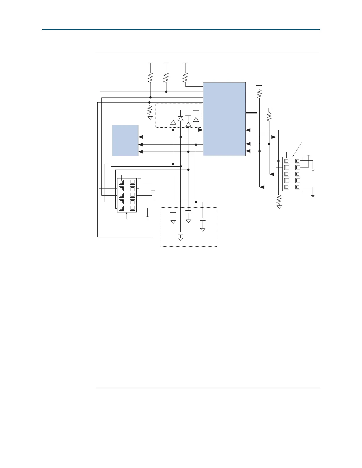
Figure 8–28. Combining JTAG and AS Configuration Schemes
Notes to Figure 8–28:
(1) Connect these pull-up resistors to the V
CCIO
supply of the bank in which the pin resides.
(2) Power up the V
CC
of the EthernetBlaster, ByteBlaster II, or USB-Blaster cable with the 3.3-V supply.
(3) Pin 6 of the header is a V
IO
reference voltage for the MasterBlaster output driver.The V
IO
must match the V
CCA
of the
device. For this value, refer to the MasterBlaster Serial/USB Communications Cable User Guide. When using the
ByteBlasterMV download cable, this pin is a no connect. When using the USB-Blaster and ByteBlaster II cables, this
pin is connected to
nCE
when it is used for AS programming, otherwise it is a no connect.
(4) The
MSEL
pin settings vary for different configuration voltage standards and POR time. To connect
MSEL
for AS
configuration schemes, refer to Table 8–3 on page 8–8, Table 8–4 on page 8–8, and Table 8–5 on page 8–9. Connect
the
MSEL
pins directly to V
CCA
or GND.
(5) Power up the V
CC
of the EthernetBlaster, ByteBlaster II, USB-Blaster, or ByteBlasterMV cable with a 2.5-V V
CCA
supply.
Third-party programmers must switch to 2.5 V. Pin 4 of the header is a V
CC
power supply for the MasterBlaster cable.
The MasterBlaster cable can receive power from either 5.0- or 3.3-V circuit boards, DC power supply, or 5.0 V from
the USB cable. For this value, refer to the MasterBlaster Serial/USB Communications Cable User Guide.
(6) You must place the diodes and capacitors as close as possible to the Cyclone IV device. Altera recommends using
the Schottky diode, which has a relatively lower forward diode voltage (VF) than the switching and Zener diodes, for
effective voltage clamping.
(7) These pins are dual-purpose I/O pins. The
nCSO
pin functions as
FLASH_nCE
pin in AP mode. The
ASDO
pin functions
as
DATA[1]
pin in AP and FPP modes.
(8) Resistor value can vary from 1 k to 10 k..
(9) Only Cyclone IV GX devices have an option to select
CLKUSR
(40 MHz maximum) as the external clock source for
DCLK
.
DATA
DCLK
nCS
ASDI
Serial
Configuration
Device
Cyclone IV Device
10 kΩ10 kΩ
V
CCIO
V
CCIO
GND
nCEO
nCE
nSTATUS
CONF_DONE
10 kΩ
V
CCIO
nCONFIG
MSEL[ ]
(1) (1) (1)
(4)
10kΩ
V
CCA
N.C.
V
CCA
TCK
TDO
TMS
TDI
CLKUSR
(9)
GND
V
CCA
(5)
V
IO
(3)
3.3 V
(2)
Pin 1
Pin 1
Download Cable
(JTAG Mode)
10-Pin Male Header
(top view)
Download Cable
(AS Mode)
10-Pin Male Header
3.3 V
10 pf
GND
GND
10 pf
10 pf
GND
10 pf
GND
(6)
(6)
(8)
(8)
3.3 V
3.3 V
3.3 V
DATA[0]
DCLK
nCSO (7)
ASDO (7)
1 kΩ