Chapter 1: Cyclone IV Transceivers Architecture 1–13
Receiver Channel Datapath
February 2015 Altera Corporation Cyclone IV Device Handbook,
Volume 2
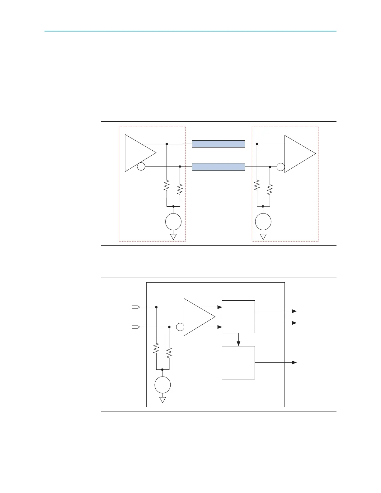
In a DC-coupled link, the transmitter DC common mode voltage is seen unblocked at
the receiver input buffer as shown in Figure 1–13. The link common mode voltage
depends on the transmitter common mode voltage and the receiver common mode
voltage. When using the receiver OCT and on-chip biasing circuitry in a DC coupled
link, you must ensure the transmitter common mode voltage is compatible with the
receiver common mode requirements. If you disable the OCT, you must terminate and
bias the receiver externally and ensure compatibility between the transmitter and the
receiver common mode voltage.
Figure 1–14 shows the receiver input buffer block diagram.
The receiver input buffers support the following features:
Figure 1–13. DC-Coupled Link with OCT
Figure 1–14. Receiver Input Buffer Block Diagram
Transmitter
Receiver
TX
V
CM
RX
V
CM
TX Termination
RX Termination
Physical Medium
Physical Medium
Receiver Input Buffer
Equalization
and
DC Gain
Circuitry
To CDRrx_datain
Signal
Detect
Signal
Threshold
Detection
Circuitry
RX
V
CM
50 or 75
50 or 75