Port Integration Module (S12GPIMV1)
MC9S12G Family Reference Manual Rev.1.27
NXP Semiconductors 221
2.4.3.35 Port P Input Register (PTIP)
Table 2-61. PTP Register Field Descriptions
Field Description
7-0
PTP
Port P general-purpose input/output data—Data Register
When not used with an alternative signal, the associated pin can be used as general-purpose I/O. In general-purpose
output mode the port data register bit value is driven to the pin.
If the associated data direction bit is set to 1, a read returns the value of the port data register bit, otherwise the
buffered pin input state is read.
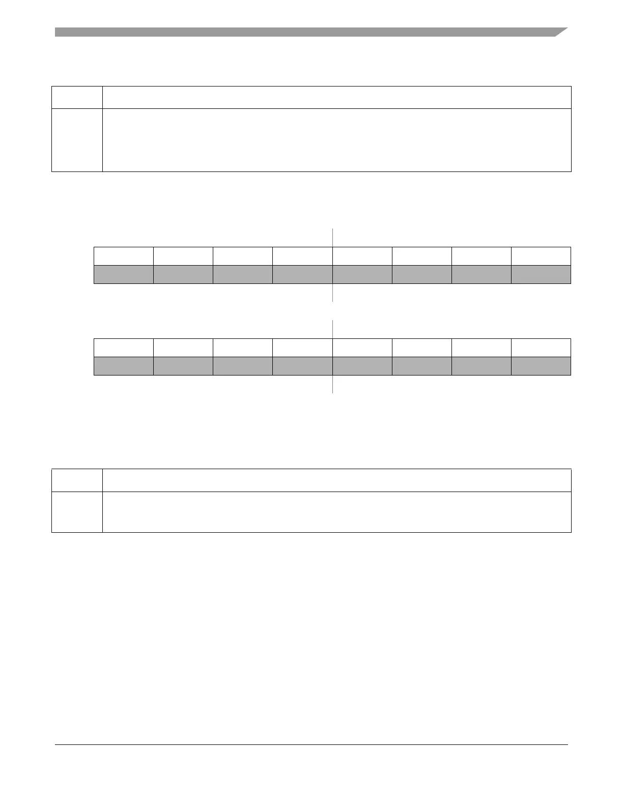
Address 0x0259 (G1, G2) Access: User read only
1
1
Read: Anytime
Write:Never
76543210
R PTIP7 PTIP6 PTIP5 PTIP4 PTIP3 PTIP2 PTIP1 PTIP0
W
Reset00000000
Address 0x0259 (G3) Access: User read only
1
76543210
R 0 0 PTIP5 PTIP4 PTIP3 PTIP2 PTIP1 PTIP0
W
Reset00000000
Figure 2-36. Port P Input Register (PTIP)
Table 2-62. PTIP Register Field Descriptions
Field Description
7-0
PTIP
Port P input data—
A read always returns the buffered input state of the associated pin. It can be used to detect overload or short circuit
conditions on output pins.

 Loading...


