Chapter 8: Configuration and Remote System Upgrades in Cyclone IV Devices 8–11
Configuration
May 2013 Altera Corporation Cyclone IV Device Handbook,
Volume 1
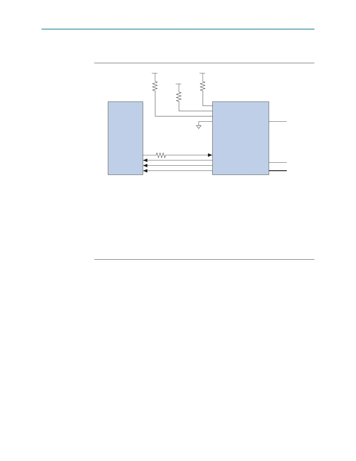
This four-pin interface connects to Cyclone IV device pins, as shown in Figure 8–2.
1 To tri-state the configuration bus for AS configuration schemes, you must tie
nCE
high
and
nCONFIG
low.
1 The 25- resistor at the near end of the serial configuration device for
DATA[0]
works
to minimize the driver impedance mismatch with the board trace and reduce the
overshoot seen at the Cyclone IV device
DATA[0]
input pin.
In the single-device AS configuration, the maximum board loading and board trace
length between the supported serial configuration device and the Cyclone IV device
must follow the recommendations in Table 8–7 on page 8–18.
The
DCLK
generated by the Cyclone IV device controls the entire configuration cycle
and provides timing for the serial interface. Cyclone IV devices use an internal
oscillator or an external clock source to generate the
DCLK
. For Cyclone IV E devices,
you can use a 40-MHz internal oscillator to generate the
DCLK
and for Cyclone IV GX
devices you can use a slow clock (20 MHz maximum) or a fast clock
(40 MHz maximum) from the internal oscillator or an external clock from
CLKUSR
to
generate the
DCLK
. There are some variations in the internal oscillator frequency
because of the process, voltage, and temperature (PVT) conditions in Cyclone IV
Figure 8–2. Single-Device AS Configuration
Notes to Figure 8–2:
(1) Connect the pull-up resistors to the V
CCIO
supply of the bank in which the pin resides.
(2) Cyclone IV devices use the
ASDO
-to-
ASDI
path to control the configuration device.
(3) The
nCEO
pin is left unconnected or used as a user I/O pin when it does not feed the
nCE
pin of another device.
(4) The
MSEL
pin settings vary for different configuration voltage standards and POR time. To connect the
MSEL
pins,
refer to Table 8–3 on page 8–8, Table 8–4 on page 8–8, and Table 8–5 on page 8–9. Connect the
MSEL
pins directly
to V
CCA
or GND.
(5) Connect the series resistor at the near end of the serial configuration device.
(6) These pins are dual-purpose I/O pins. The
nCSO
pin functions as
FLASH_nCE
pin in AP mode. The
ASDO
pin functions
as the
DATA[1]
pin in AP and FPP modes.
(7) Only Cyclone IV GX devices have an option to select
CLKUSR
(40 MHz maximum) as the external clock source for
DCLK
.
nSTATUS
nCONFIG
CONF_DONE
nCE
DATA[0]
DCLK
nCSO (6)
ASDO (6)
nCEO
MSEL[ ]
DATA
DCLK
nCS
ASDI
V
CCIO
(1)
GND
10 kΩ
V
CCIO
(1)
10 kΩ
V
CCIO
(1)
10 kΩ
N.C. (3
(4)
CLKUSR
(7)
(2)
25 Ω (5)
Serial Configuration
Device
Cyclone IV Device