Chapter 8: Configuration and Remote System Upgrades in Cyclone IV Devices 8–17
Configuration
May 2013 Altera Corporation Cyclone IV Device Handbook,
Volume 1
Single SRAM Object File
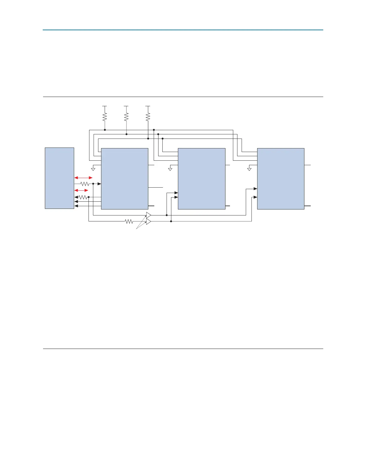
The second method configures both the master device and slave devices with the
same .sof. The serial configuration device stores one copy of the .sof. You must set up
one or more slave devices in the chain. All the slave devices must be set up in the
same way (Figure 8–5).
In this setup, all the Cyclone IV devices in the chain are connected for concurrent
configuration. This reduces the AS configuration time because all the Cyclone IV
devices are configured in one configuration cycle. Connect the
nCE
input pins of all the
Cyclone IV devices to GND. You can either leave the
nCEO
output pins on all the
Cyclone IV devices unconnected or use the
nCEO
output pins as normal user I/O pins.
The
DATA
and
DCLK
pins are connected in parallel to all the Cyclone IV devices.
Figure 8–5. Multi-Device AS Configuration in Which Devices Receive the Same Data with a Single .sof
Notes to Figure 8–5:
(1) Connect the pull-up resistors to the V
CCIO
supply of the bank in which the pin resides.
(2) The
nCEO
pin is left unconnected or used as a user I/O pin when it does not feed the
nCE
pin of another device.
(3) The
MSEL
pin settings vary for different configuration voltage standards and POR time. You must set the master device of the Cyclone IV device
in AS mode and the slave devices in PS mode. To connect the
MSEL
pins for the master device in AS mode and slave devices in PS mode, refer to
Table 8–3 on page 8–8, Table 8–4 on page 8–8, and Table 8–5 on page 8–9. Connect the
MSEL
pins directly to V
CCA
or GND.
(4) Connect the series resistor at the near end of the serial configuration device.
(5) Connect the repeater buffers between the master and slave devices for
DATA[0]
and
DCLK
. All I/O inputs must maintain a maximum AC voltage
of 4.1 V. The output resistance of the repeater buffers must fit the maximum overshoot equation outlined in “Configuration and JTAG Pin I/O
Requirements” on page 8–5.
(6) The 50- series resistors are optional if the 3.3-V configuration voltage standard is applied. For optimal signal integrity, connect these 50- series
resistors if the 2.5- or 3.0-V configuration voltage standard is applied.
(7) These pins are dual-purpose I/O pins. The
nCSO
pin functions as
FLASH_nCE
pin in AP mode. The
ASDO
pin functions as
DATA[1]
pin in AP and
FPP modes.
(8) Only Cyclone IV GX devices have an option to select
CLKUSR
(40 MHz maximum) as the external clock source for
DCLK
.
(9) For multi-devices AS configuration using Cyclone IV E with 1,0 V core voltage, the maximum board trace-length from the serial configuration
device to the junction-split on both
DCLK
and
Data0
line is 3.5 inches.
nSTATUS
nCONFIG
CONF_DONE
nCE
DATA[0]
DCLK
nCEO
N.C. (2)
(3)
nSTATUS
nCONFIG
CONF_DONE
nCE
DATA[0]
DCLK
nCEO
N.C. (2)
(3)
nSTATUS
nCONFIG
CONF_DONE
nCE
DATA[0]
DCLK
nCSO (7)
ASDO (7)
nCEO
MSEL[ ]
(3) MSEL[ ] MSEL[ ]
DATA
DCLK
nCS
ASDI
Serial Configuration
Device
GND GNDGND
N.C. (2)
V
CCIO
(1) V
CCIO
(1) V
CCIO
(1)
Buffers (5)
10 k
Ω 10 kΩ 10 kΩ
(4)
25
Ω
(7)
50 Ω
(4),(6)
50
Ω
Cyclone IV Slave Device 2
Cyclone IV Slave Device 1
Cyclone IV Master Device
CLKUSR
(9)
(9)
(9)