8–38 Chapter 8: Configuration and Remote System Upgrades in Cyclone IV Devices
Configuration
Cyclone IV Device Handbook, May 2013 Altera Corporation
Volume 1
The programming hardware or download cable then places the configuration data
one bit at a time on the
DATA[0]
pin of the device. The configuration data is clocked
into the target device until
CONF_DONE
goes high. The
CONF_DONE
pin must have an
external 10-k pull-up resistor for the device to initialize.
When you use a download cable, setting the Auto-restart configuration after error
option does not affect the configuration cycle because you must manually restart
configuration in the Quartus II software if an error occurs. Additionally, the Enable
user-supplied start-up clock (CLKUSR) option has no effect on device initialization,
because this option is disabled in the .sof when programming the device with the
Quartus II Programmer and download cable. Therefore, if you turn on the CLKUSR
option, you do not have to provide a clock on
CLKUSR
when you configure the device
with the Quartus II Programmer and a download cable.
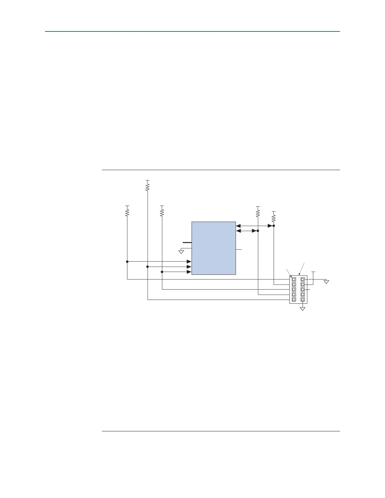
Figure 8–17 shows PS configuration for Cyclone IV devices with a download cable.
Figure 8–17. PS Configuration Using a Download Cable
Notes to Figure 8–17:
(1) You must connect the pull-up resistor to the same supply voltage as the V
CCA
supply.
(2) The pull-up resistors on
DATA[0]
and
DCLK
are only required if the download cable is the only configuration scheme
used on your board. This is to ensure that
DATA[0]
and
DCLK
are not left floating after configuration. For example,
if you also use a configuration device, the pull-up resistors on
DATA[0]
and
DCLK
are not required.
(3) Pin 6 of the header is a V
IO
reference voltage for the MasterBlaster output driver. V
IO
must match the V
CCA
of the
device. For this value, refer to the MasterBlaster Serial/USB Communications Cable User Guide. With the USB-Blaster,
ByteBlaster II, ByteBlaster MV, and EthernetBlaster, this pin is a no connect.
(4) The
nCEO
pin is left unconnected or used as a user I/O pin when it does not feed the
nCE
pin of another device.
(5) The
MSEL
pin settings vary for different configuration voltage standards and POR time. To connect the
MSEL
pins,
refer to Table 8–3 on page 8–8, Table 8–4 on page 8–8, and Table 8–5 on page 8–9 for PS configuration schemes.
Connect the
MSEL
pins directly to V
CCA
or GND.
(6) Power up the V
CC
of the ByteBlaster II, USB-Blaster, or ByteBlasterMV cable with a 2.5-V supply from V
CCA
.
Third-party programmers must switch to 2.5 V. Pin 4 of the header is a V
CC
power supply for the MasterBlaster cable.
The MasterBlaster cable can receive power from either 5.0- or 3.3-V circuit boards, DC power supply, or 5.0 V from
the USB cable. For this value, refer to the MasterBlaster Serial/USB Communications Cable User Guide.
MSEL[ ] (5)
nCONFIG
CONF_DONE
V
CCA
(1)
V
CCA
(6)
Shield
GND
V
CCA
(1)
GND
V
CCA
(1)
10 kΩ
10 kΩ
V
CCA
(1)
10 kΩ
10 kΩ
nSTATUS
Pin 1
Download Cable 10-Pin Male
Header (Top View)
GND
V
IO
(3)
Cyclone IV Device
nCEO
DCLK
DATA[0]
nCE
V
CCA
(1)
N.C. (4)
(2)
(2)
10 kΩ