8–50 Chapter 8: Configuration and Remote System Upgrades in Cyclone IV Devices
Configuration
Cyclone IV Device Handbook, May 2013 Altera Corporation
Volume 1
When programming a JTAG device chain, one JTAG-compatible header is connected
to several devices. The number of devices in the JTAG chain is limited only by the
drive capability of the download cable. When four or more devices are connected in a
JTAG chain, Altera recommends buffering the
TCK
,
TDI
, and
TMS
pins with an on-board
buffer.
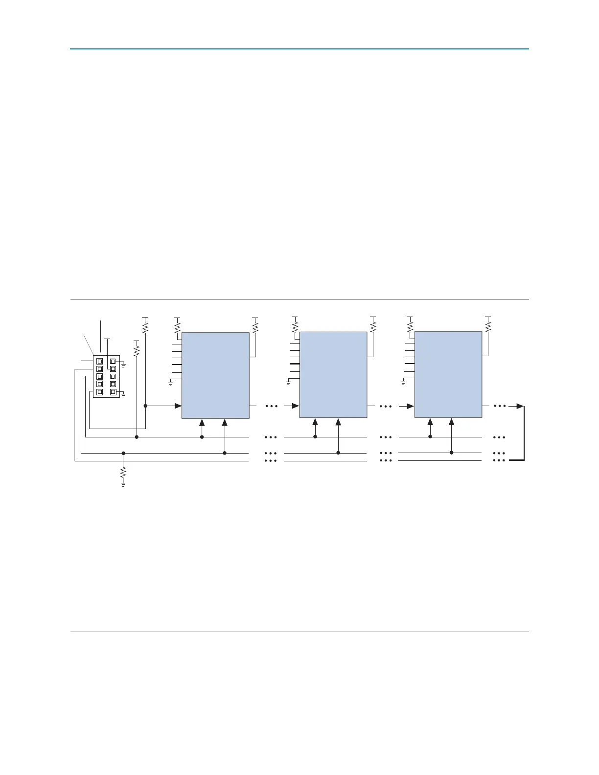
JTAG-chain device programming is ideal when the system contains multiple devices,
or when testing your system with JTAG BST circuitry. Figure 8–25 and Figure 8–26
show multi-device JTAG configuration.
For devices using 2.5-, 3.0-, and 3.3-V V
CCIO
supply, you must refer to Figure 8–25. All
I/O inputs must maintain a maximum AC voltage of 4.1 V because JTAG pins do not
have the internal PCI clamping diodes to prevent voltage overshoot when using 2.5-,
3.0-, and 3.3- V V
CCIO
supply. You must power up the V
CC
of the download cable with
a 2.5-V V
CCA
supply. For device using V
CCIO
of 1.2, 1.5 V, and 1.8 V, refer to
Figure 8–26. You can power up the V
CC
of the download cable with the supply from
V
CCIO
.
Figure 8–25. JTAG Configuration of Multiple Devices Using a Download Cable (2.5, 3.0, and 3.3-V V
CCIO
Powering the
JTAG Pins)
Notes to Figure 8–25:
(1) Connect these pull-up resistors to the V
CCIO
supply of the bank in which the pin resides.
(2) Connect the
nCONFIG
and
MSEL
pins to support a non-JTAG configuration scheme. If you only use a JTAG configuration, connect the
nCONFIG
pin to logic-high and the
MSEL
pins to GND. In addition, pull
DCLK
and
DATA[0]
to either high or low, whichever is convenient on your board.
(3) Pin 6 of the header is a V
IO
reference voltage for the MasterBlaster output driver. V
IO
must match the V
CCA
of the device. For this value, refer to the
MasterBlaster Serial/USB Communications Cable User Guide. In the ByteBlasterMV cable, this pin is a no connect. In the USB-Blaster and
ByteBlaster II cables, this pin is connected to
nCE
when it is used for AS programming, otherwise it is a no connect.
(4) You must connect the
nCE
pin to GND or driven low for successful JTAG configuration.
(5) Power up the V
CC
of the ByteBlaster II, USB-Blaster, or ByteBlasterMV cable with a 2.5-V supply from V
CCA
. Third-party programmers must switch
to 2.5 V. Pin 4 of the header is a V
CC
power supply for the MasterBlaster cable. The MasterBlaster cable can receive power from either 5.0- or 3.3-V
circuit boards, DC power supply, or 5.0 V from the USB cable. For this value, refer to the MasterBlaster Serial/USB Communications Cable User
Guide.
(6) Resistor value can vary from 1 k to 10 k.
TMS TCK
Download Cable
10-Pin Male Header
TDI
TDO
Pin 1
nST
A
TUS
nCONFIG
nCE
(4)
CONF_DONE
VCCIO
(2)
(2)
VIO
(3)
(6)
(6)
(1) (1)
(2)
DATA[0]
DCLK
(2)
MSEL[ ]
nCEO
(2)
TMS TCK
TDI
TDO
nST
A
TUS
nCONFIG
nCE
(4)
CONF_DONE
(2)
(2)
(1)
(2)
DATA[0]
DCLK
(2)
nCEO
(2)
(1)
TMS TCK
TDI
TDO
nST
A
TUS
nCONFIG
nCE
(4)
V
CCIO
V
CCIO
V
CCIO
V
CCIO
V
CCA
V
CCA
CONF_DONE
(2)
(2)
(2)
DATA[0]
DCLK
(2)
nCEO
(2)
(1)
(1)
10 kΩ
10 kΩ
10 kΩ
10 kΩ
10 kΩ
10 kΩ
Cyclone IV Device
Cyclone IV Device Cyclone IV Device
V
CCIO
(5)
MSEL[ ]
MSEL[ ]
V
CCA
1 kΩ