Chapter 1: Cyclone IV Transceivers Architecture 1–35
Transceiver Clocking Architecture
February 2015 Altera Corporation Cyclone IV Device Handbook,
Volume 2
When the byte serializer is enabled, the low-speed clock frequency is halved before
feeding into the read clock of TX phase compensation FIFO. The low-speed clock is
available in the FPGA fabric as
tx_clkout
port, which can be used in the FPGA fabric
to send transmitter data and control signals.
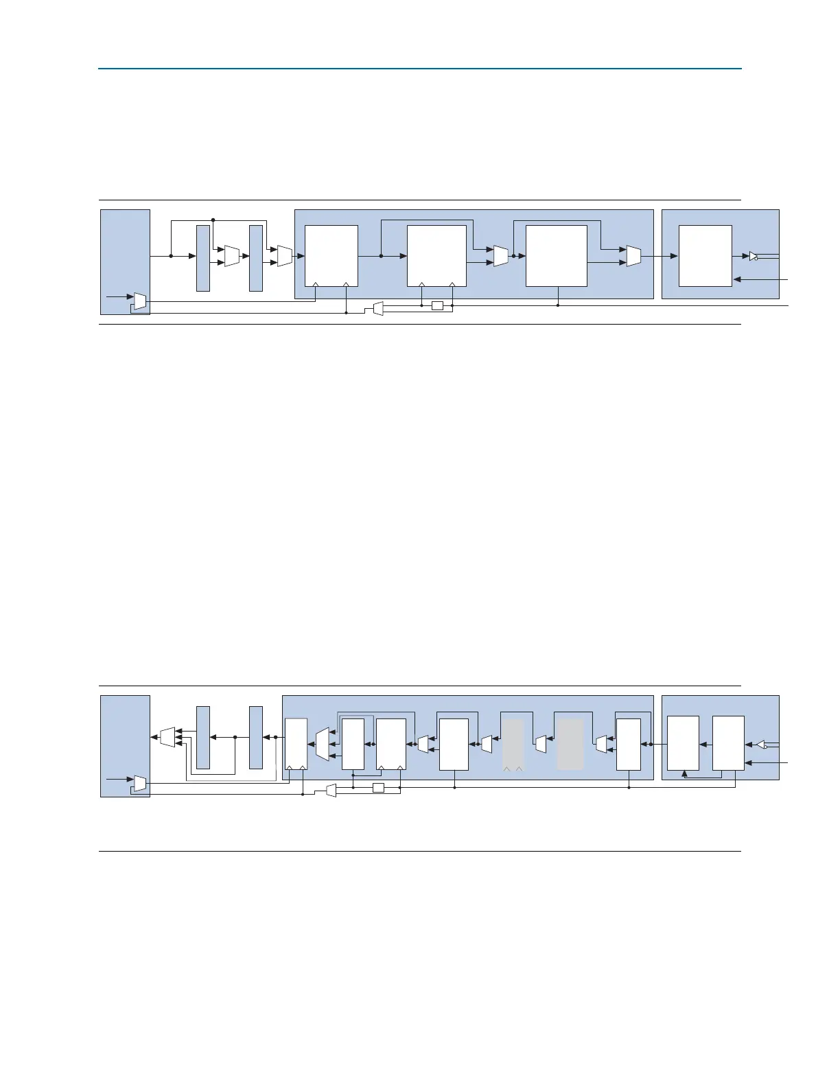
Figure 1–34 shows the datapath clocking in receiver only operation. In this mode, the
receiver PCS supports configuration without the rate match FIFO. The CDR unit in
the channel recovers the clock from the received serial data and generates the high-
speed recovered clock for the deserializer, and low-speed recovered clock for
forwarding to the receiver PCS. The low-speed recovered clock feeds to the following
blocks in the receiver PCS:
■ word aligner
■ 8B/10B decoder
■ write clock of byte deserializer
■ byte ordering
■ write clock of RX phase compensation FIFO
When the byte deserializer is enabled, the low-speed recovered clock frequency is
halved before feeding into the write clock of the RX phase compensation FIFO. The
low-speed recovered clock is available in the FPGA fabric as
rx_clkout
port, which
can be used in the FPGA fabric to capture receiver data and status signals.
When the transceiver is configured for transmitter and receiver operation in
non-bonded channel configuration, the receiver PCS supports configuration with and
without the rate match FIFO. The difference is only at the receiver datapath clocking.
The transmitter datapath clocking is identical to transmitter only operation mode as
shown in Figure 1–33.
Figure 1–33. Transmitter Only Datapath Clocking in Non-Bonded Channel Configuration
Byte Serializer
8B/10B Encoder
Transmitter Channel PCS Transmitter Channel PMA
Serializer
PCIe Hard IP
FPGA
Fabric
PIPE Interface
Tx Phase
Comp
FIFO
tx_datain
tx_dataout
wr_clk rd_clk wr_clk rd_clk
high-speed
clock
low-speed clock
tx_coreclk
tx_clkout
/2
Figure 1–34. Receiver Only Datapath Clocking without Rate Match FIFO in Non-Bonded Channel Configuration
Note to Figure 1–34:
(1) High-speed recovered clock.
rx_coreclk
Receiver Channel PCS Receiver Channel PMA
FPGA
Fabric
rx_dataout
rx_datain
Deserial-
izer
CDR
Byte
De-
serializer
Byte
Order-
ing
Deskew
FIFO
8B/10B
Decoder
Rate
Match
FIFO
PCIe Hard IP
PIPE Interface
CDR clock
low-speed recovered clock
rx_clkout
/2
(1)
Word
Aligner
Rx
Phase
Comp
FIFO