1–34 Chapter 1: Cyclone IV Transceivers Architecture
Transceiver Clocking Architecture
Cyclone IV Device Handbook, February 2015 Altera Corporation
Volume 2
The transceiver datapath clocking varies in non-bonded channel configuration
depending on the PCS configuration.
Figure 1–33 shows the datapath clocking in transmitter only operation. In this mode,
each channel selects the high- and low-speed clock from one of the supported PLLs.
The high-speed clock feeds to the serializer for parallel to serial operation. The
low-speed clock feeds to the following blocks in the transmitter PCS:
■ 8B/10B encoder
■ read clock of the byte serializer
■ read clock of the TX phase compensation FIFO
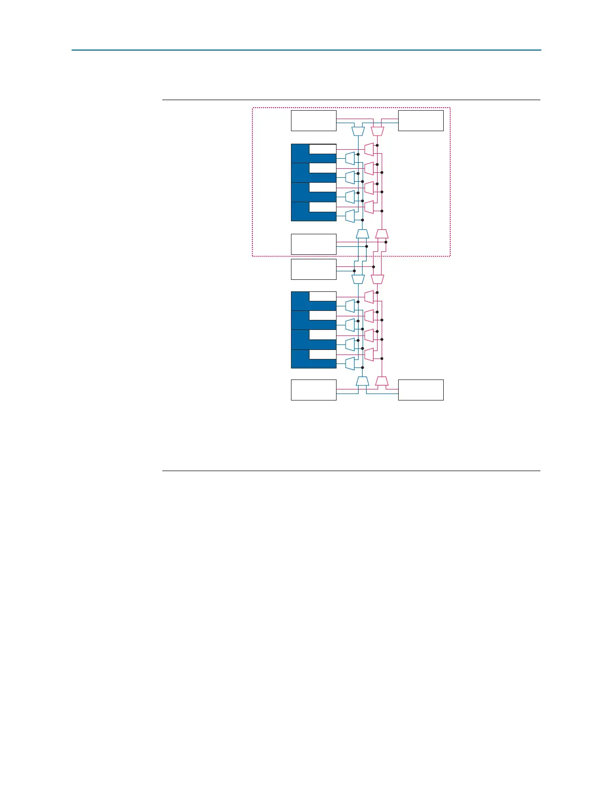
Figure 1–32. Clock Distribution in Non-Bonded Channel Configuration for Transceivers in F484
and Larger Packages
Notes to Figure 1–32:
(1) High-speed clock.
(2) Low-speed clock.
(3) These PLLs have restricted clock driving capability and may not reach all connected channels. For details, refer to
Table 1–9.
Not applicable in
F484 package
Transceiver
Block
GXBL1
MPLL_8
TX PMA
TX PMA
TX PMA
TX PMA
Ch3
MPLL_7
Ch2
Ch3
Ch2
Ch1
Ch0
(1)
(2)
(1)
(2)
Transceiver
Block
GXBL0
MPLL_6
TX PMA
TX PMA
TX PMA
TX PMA
MPLL_5
GPLL_2
GPLL_1
Ch1
Ch0
(3)
(3)
(3)
(3)