4–2 Altera Corporation
Stratix Device Handbook, Volume 2 June 2006
Stratix & Stratix GX I/O Standards
3.3-V Low Voltage Transistor-Transistor Logic (LVTTL) -
EIA/JEDEC Standard JESD8-B
The 3.3-V LVTTL I/O standard is a general-purpose, single-ended
standard used for 3.3-V applications. The LVTTL standard defines the DC
interface parameters for digital circuits operating from a 3.0-V or 3.3-V
power supply and driving or being driven by LVTTL-compatible devices.
The LVTTL input standard specifies a wider input voltage range of
–0.5 V ≤V
I
≤3.8 V. Altera allows an input voltage range of –0.5 V ≤V
I
≤4.1
V. The LVTTL standard does not require input reference voltages or board
terminations.
Stratix and Stratix GX devices support both input and output levels for
3.3-V LVTTL operation.
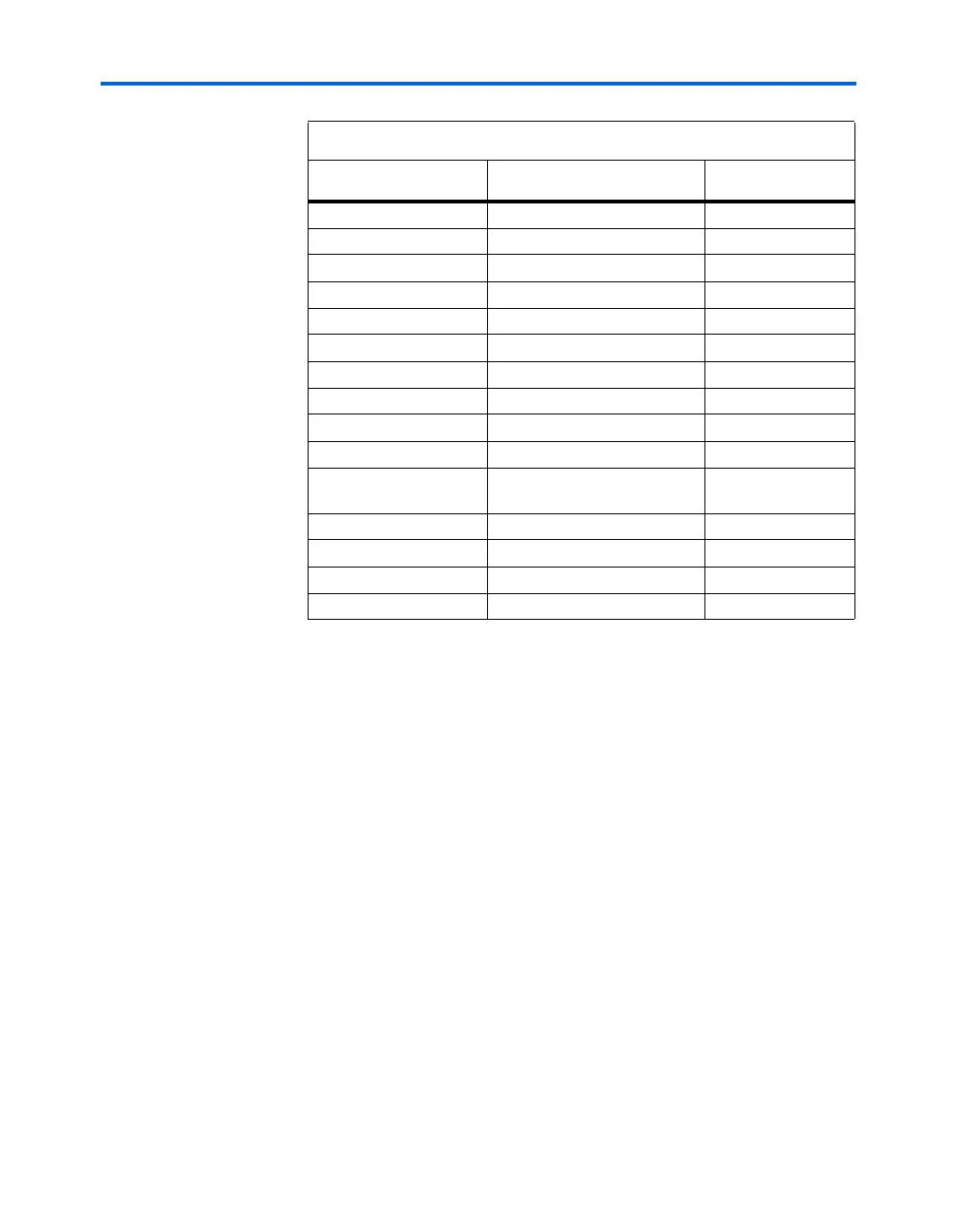
PCI-X 1.0 PC/embedded systems 133 MHz
AGP 1× and 2× Graphics processors 66 to 133 MHz
SSTL-3 Class I and II SDRAM 167 MHz
SSTL-2 Class I and II DDR I SDRAM 160 to 400 Mbps
HSTL Class I QDR SRAM/SRAM/CSIX 150 to 225 MHz
HSTL Class II QDR SRAM/SRAM/CSIX 150 to 250 MHz
Differential HSTL Clock interfaces 150 to 225 MHz
GTL Backplane driver 200 MHz
GTL+ Pentium processor interface 133 to 200 MHz
LVDS Communications 840 Mbps
HyperTransport
technology
Motherboard interfaces 800 Mbps
LVPECL PHY interface 840 Mbps
PCML Communications 840 Mbps
Differential SSTL-2 DDR I SDRAM 160 to 400 Mbps
CTT Back planes and bus interfaces 200 MHz
Note to Ta b le 4 – 1 :
(1) These performance values are dependent on device speed grade, package type
(flip-chip or wirebond) and location of I/Os (top/bottom or left/right). See the
DC & Switching Characteristics chapter of the Stratix Device Handbook, Volume 1.
Table 4–1. I/O Standard Applications & Performance (Part 2 of 2) Note (1)
I/O Standard Application Performance