13–10 Altera Corporation
Stratix Device Handbook, Volume 2 July 2005
Package Outlines
956-Pin Ball Grid Array (BGA) - Flip Chip
■ All dimensions and tolerances conform to ASME Y14.5M - 1994.
■ Controlling dimension is in millimeters.
■ Pin A1 may be indicated by an ID dot, or a special feature, in its
proximity on package surface.
Tables 13–9 and 13–10 show the package information and package
outline figure references, respectively, for the 956-pin BGA packaging.
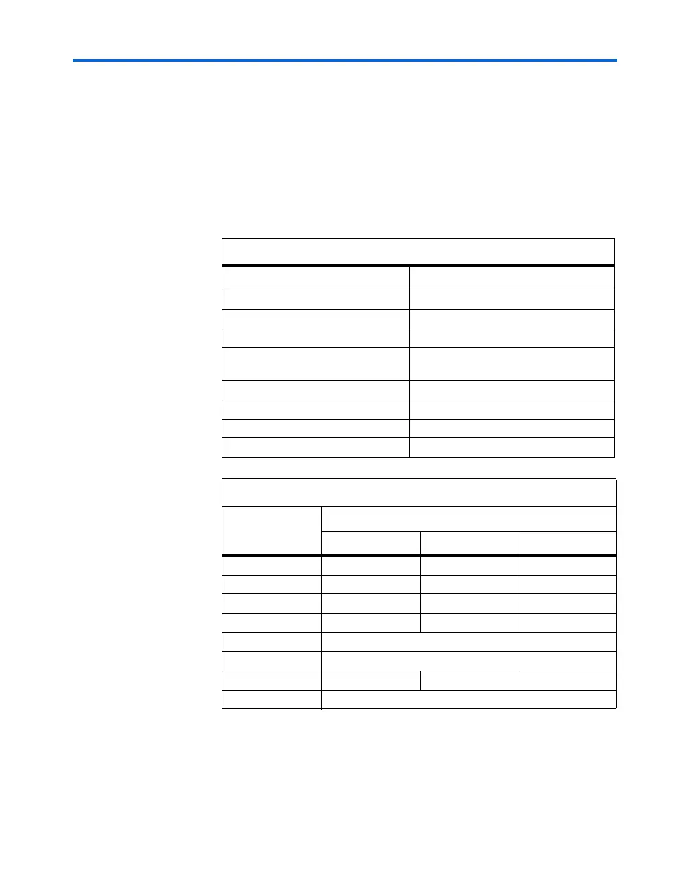
Table 13–9. 956-Pin BGA Package Information
Description Specification
Ordering code reference B
Package acronym BGA
Substrate material BT
Solder ball composition Regular: 63Sn:37Pb (Typ.)
Pb-free: Sn:3Ag:0.5Cu (Typ.)
JEDEC outline reference MS-034 Variation: BAU-1
Maximum lead coplanarity 0.008 inches (0.20 mm)
Weight 14.6 g
Moisture sensitivity level Printed on moisture barrier bag
Table 13–10. 956-Pin BGA Package Outline Dimensions
Symbol
Millimeters
Min. Nom. Max.
A––3.50
A1 0.30 – –
A2 0.25 – 3.00
A3 – – 2.50
D 40.00 BSC
E 40.00 BSC
b 0.60 0.75 0.90
e 1.27 BSC