Altera Corporation 4–31
June 2006 Stratix Device Handbook, Volume 2
Selectable I/O Standards in Stratix & Stratix GX Devices
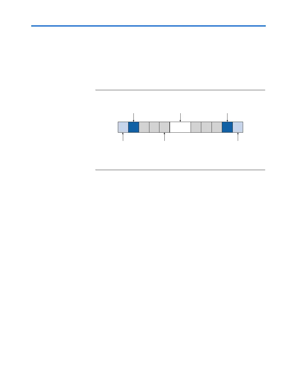
■ For flip-chip packages, there are no restrictions for placement of
single-ended input signals with respect to differential signals (see
Figure 4–21). For wire-bond packages, single ended input pads may
only be placed four or more pads away from a differential pad.
■ Single-ended outputs and bidirectional pads may only be placed five
or more pads away from a differential pad (see Figure 4–21),
regardless of package type.
Figure 4–21. Legal Pin Placement Note (1)
Note to Figure 4–21:
(1) Input pads on a flip-chip packages have no restrictions.
VREF Pad Placement Guidelines
Restrictions on the placement of single-ended voltage-referenced I/O
pads with respect to VREF pads help maintain an acceptable noise level
on the V
CCIO
supply and to prevent output switching noise from shifting
the VREF rail. The following guidelines are for placing single-ended pads
in Stratix devices.
Input Pins
Each VREF pad supports a maximum of 40 input pads with up to 20 on
each side of the VREF pad.
Output Pins
When a voltage referenced input or bidirectional pad does not exist in a
bank, there is no limit to the number of output pads that can be
implemented in that bank. When a voltage referenced input exists, each
VREF pad supports 20 outputs for thermally enhanced FineLine BGA
®
and thermally enhanced BGA cavity up packages or 15 outputs for Non-
thermally enhanced cavity up and non-thermally enhanced
FineLine BGA packages.
Differential Pin
Wirebond
Input
Input, Output,
Bidirectional
Input, Output,
Bidirectional
Input
FlipChip
Input