5–44 Altera Corporation
Stratix Device Handbook, Volume 2 July 2005
SERDES Bypass DDR Differential Signaling
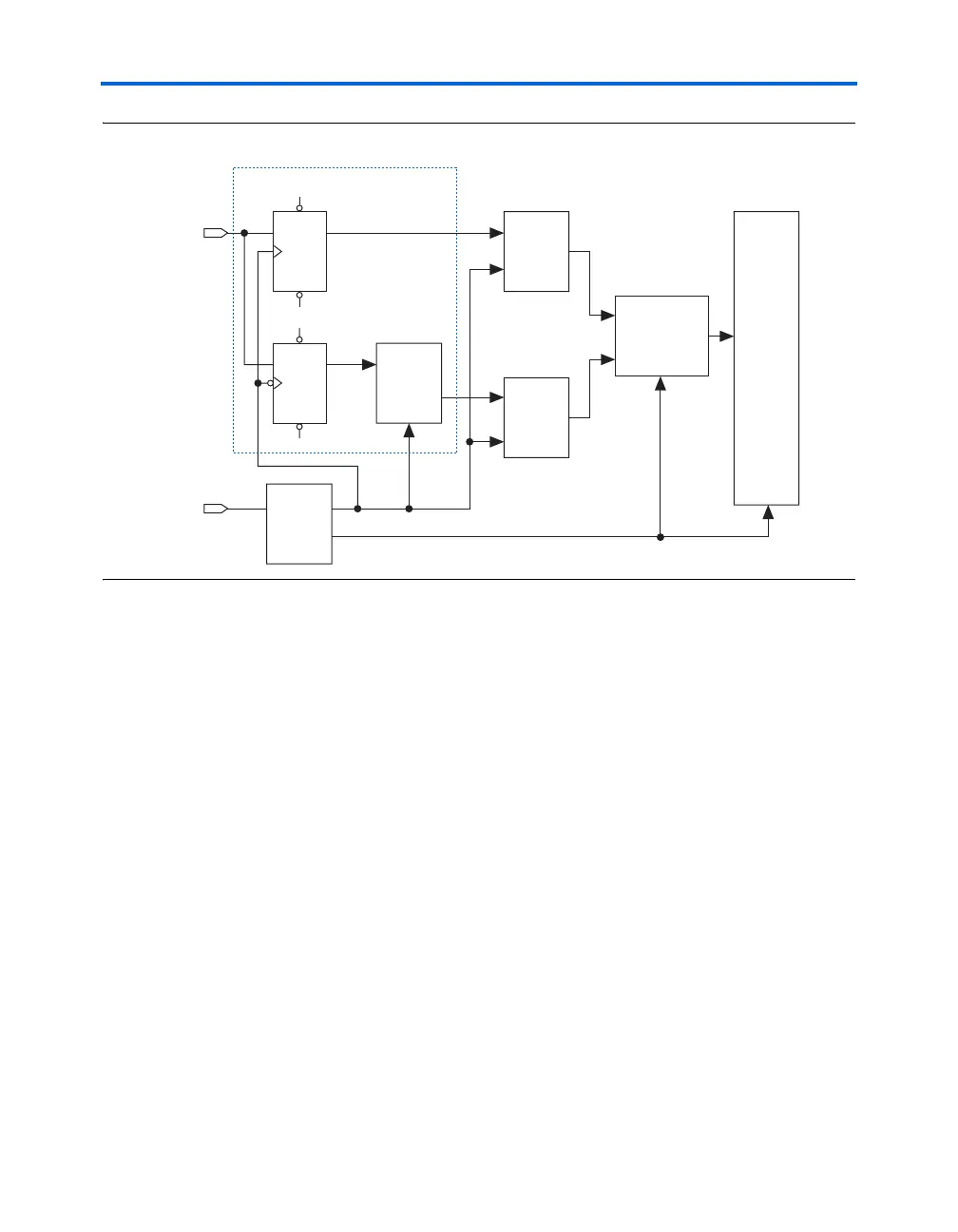
Figure 5–29. ×2 Data Rate Receiver Channel with Deserialization Factor of 8
SERDES Bypass DDR Differential Signaling Transmitter
Operation
The ×2 differential signaling transmitter uses the Stratix device DDR
output circuitry to transmit high-speed serial data. The DDR output
circuitry consists of a pair of shift registers and a multiplexer. The shift
registers capture the parallel data on the clock’s rising edge (generated by
the PLL), and a multiplexer transmits the data in sync with the clock.
Figure 5–30 shows the DDR timing relation between the parallel data and
the clock. In this example, the inclock signal is running at half the speed
of the data. However, other combinations are possible. Figure 5–31 shows
the DDR output and the other modules used in a
×2 transmitter design to
interface with the system logic.
PLL
DFF
DFF
Shift
Register
Shift
Register
Stratix
Logic
Array
inclock
datain
Latch
Register
×4
×1
Clock
DDR IOE
D0, D2, D4, D6
D1, D3, D5, D7