5–14 Altera Corporation
Stratix Device Handbook, Volume 2 July 2005
Using SERDES to Implement SDR
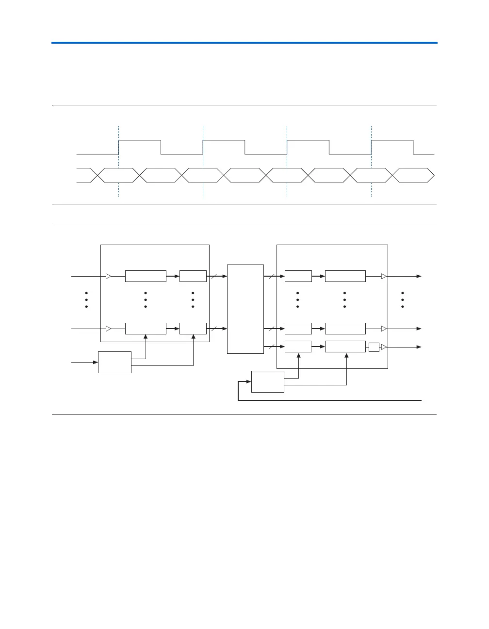
Figure 5–9 shows a DDR clock-to-data timing relationship with the clock
center-aligned with respect to data. Figure 5–10 shows the connection
between the receiver and transmitter circuits.
Figure 5–9. DDR Clock-to-Data Relationship
Figure 5–10. DDR Receiver & Transmitter Circuit Connection
Using SERDES
to Implement
SDR
Stratix devices support systems based on single data rate (SDR)
operations applications by allowing you to directly transmit out the
multiplied clock (as described in “SDR Transmitter Clock Output” on
page 5–12). These systems are usually based on Utopia-4, SFI-4, or XSBI
interfaces, and support various data rates.
An additional differential channel is automatically configured to produce
the transmitter clock output signal and is transmitted along with the data.
For example, when a system is required to transmit 10 Gbps with a 1-to-
1 clock-to-data ratio, program the SERDES with sixteen high-speed
channels running at 624 Mbps each. The Quartus II software
XX B0 A0 B1 A1 B2 A2 B3 A3
inclock
DDR
Serial-to-Parallel
Register
Parallel
Register
rx_d[0]
Channel
0
8
Parallel-to-Serial
Register
Parallel
Register
tx_d[0]
Channel
0
8
Serial-to-Parallel
Register
Parallel
Register
rx_d[15]
Channel
15
8
Parallel-to-Serial
Register
Parallel
Register
Channel
15
txclk_out
8
Parallel-to-Serial
Register
Parallel
Register
8
LVDS PLL
LVDS PLL
txloaden
rxloadena
input clock ×
W
input clock ×
W
txclk_in
100 MHz
800 Mbps
Channel
16
txclk_out
400 MHz
Stratix
Logic
Array
Stratix SERDES DDR TransmitterStratix SERDES DDR Receiver
data rate = 800 Mbps
data rate = 800 Mbps
rxclk
400 MHz
÷2