Altera Corporation 5–45
July 2005 Stratix Device Handbook, Volume 2
High-Speed Differential I/O Interfaces in Stratix Devices
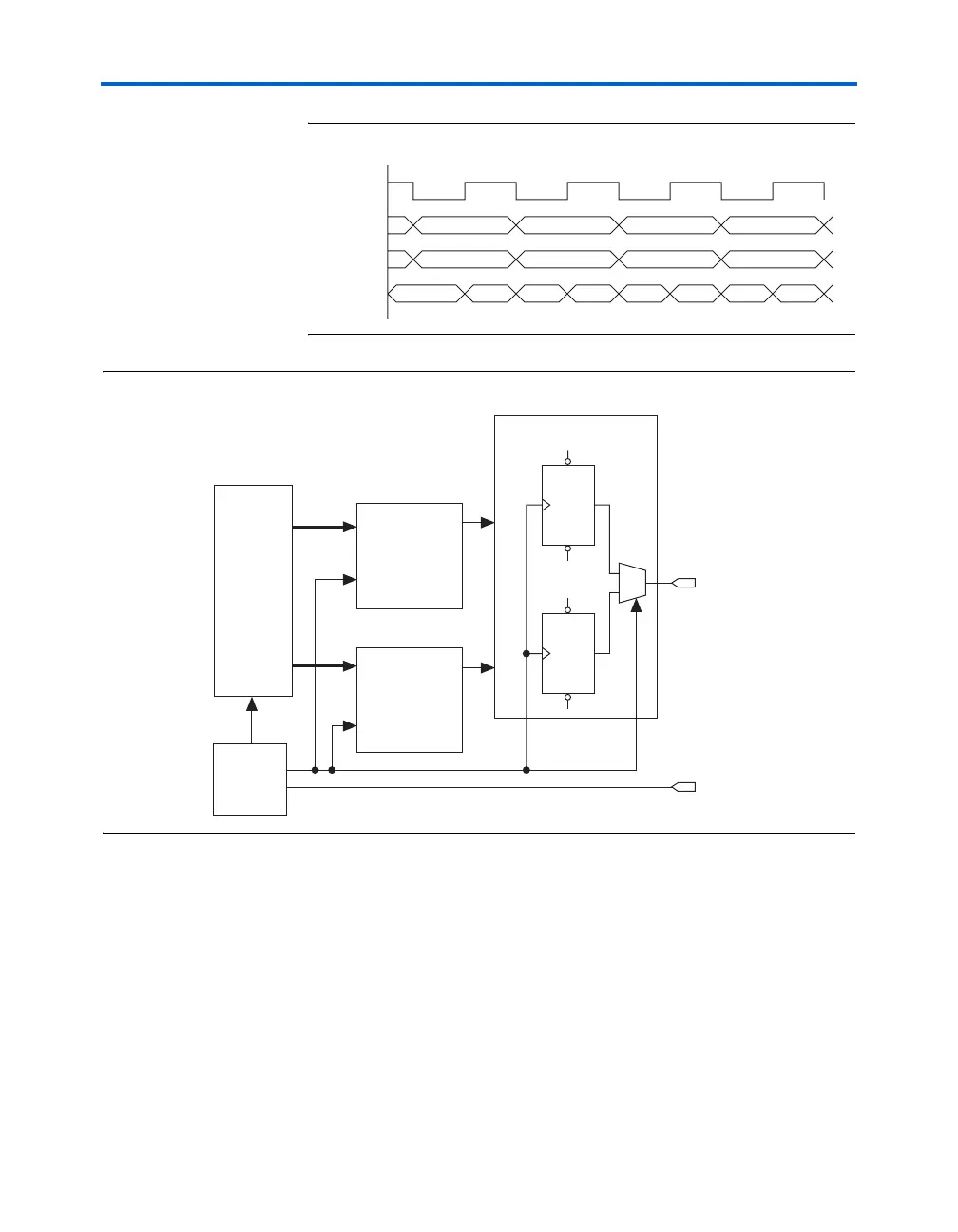
Figure 5–30. ×2 Timing Relation between Parallel Data & Clock
Figure 5–31. ×2 Data Rate Transmitter Channel with Serialization Factor of 8
High-Speed
Interface Pin
Locations
Stratix high-speed interface pins are located at the edge of the package to
limit the possible mismatch between a pair of high-speed signals. Stratix
devices have eight programmable I/O banks. Figure 5–32 shows the I/O
pins and their location relative to the package.
outclock
dataout
datain_l
datain_h
XX
XX
XX
A0 B0 A1 B1 A2 B2 A3
B0 B1 B2 B3
A0 A1 A2 A3
PLL
Stratix
Logic
Array
Shift
Register
Shift
Register
DFF
DFF
DDR IOE
inclock
dataout
D0, D2,
D4, D6
D1, D3,
D5, D7
×4
×1
×1