3–6 Altera Corporation
Stratix Device Handbook, Volume 2 June 2006
External Memory Standards
same scheme as in DDR SDRAM interfaces whereby the dedicated
circuitry is used during reads to center-align the data and the read clock
inside the FPGA and the PLL center-aligns the data and write clock
outputs. The data and clock relationship for reads and writes in
RLDRAM II is similar to those in DDR SDRAM as already depicted in
Figure 3–1 on page 3–3 and Figure 3–3 on page 3–4.
QDR & QDRII SRAM
QDR SRAM provides independent read and write ports that eliminate
the need for bus turnaround. The memory uses two sets of clocks: K and
Kn for write access, and optional C and Cn for read accesses, where Kn
and Cn are the inverse of the K and C clocks, respectively. You can use
differential HSTL I/O pins to drive the QDR SRAM clock into the Stratix
and Stratix GX devices. The separate write data and read data ports
permit a transfer rate up to four words on every cycle through the DDR
circuitry. Stratix and Stratix GX devices support both burst-of-two and
burst-of-four QDR SRAM architectures, with clock cycles up to 167 MHz
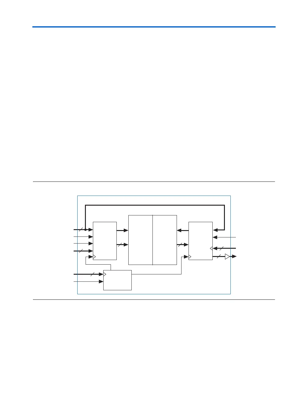
using the 1.5-V HSTL Class I or Class II I/O standard. Figure 3–4 shows
the block diagram for QDR SRAM burst-of-two architecture.
Figure 3–4. QDR SRAM Block Diagram for Burst-of-Two Architecture
QDRII SRAM is a second generation of QDR SRAM devices. It can
transfer four words per clock cycle, fulfilling the requirements facing
next-generation communications system designers. QDRII SRAM
devices provide concurrent reads and writes, zero latency, and increased
data throughput. Stratix and Stratix GX devices support QDRII SRAM at
speeds up to 200 MHz since the timing requirements for QDRII SRAM
are not as strict as QDR SRAM.
256K × 18
Memory
Array
256K × 18
Memory
Array
Read
Port
RPSn
Q
Write
Port
WPSn
D
A
18
18
Data
Control
Logic
K, Kn
18
36
BWSn
V
REF
C, Cn
2
2
Data
36
Discrete QDR SRAM Device