5–50 Altera Corporation
Stratix Device Handbook, Volume 2 July 2005
Board Design Consideration
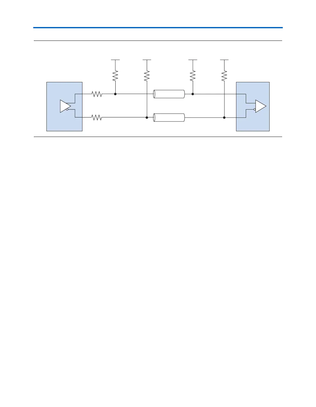
Figure 5–39. Differential SSTL-2 Class II Termination
Board Design
Consideration
This section is a brief explanation of how to get the optimal performance
from the Stratix high-speed I/O block and ensure first-time success in
implementing a functional design with optimal signal quality. For more
information on detailed board layout recommendation and I/O pin
terminations see AN 224: High-Speed Board Layout Guidelines.
You must consider the critical issues of controlled impedance of traces
and connectors, differential routing, and termination techniques to get
the best performance from the IC. For more information, use this chapter
and the Stratix Device Family Data Sheet section of the Stratix Device
Handbook, Volume 1.
The Stratix high-speed module generates signals that travel over the
media at frequencies as high as 840 Mbps. Board designers should use the
following general guidelines:
■ Baseboard designs on controlled differential impedance. Calculate
and compare all parameters such as trace width, trace thickness, and
the distance between two differential traces.
■ Place external reference resistors as close to receiver input pins as
possible.
■ Use surface mount components.
■ Avoid 90° or 45° corners.
■ Use high-performance connectors such as HS-3 connectors for
backplane designs. High-performance connectors are provided by
Teradyne Corp (www.teradyne.com) or Tyco International Ltd.
(www.tyco.com).
■ Design backplane and card traces so that trace impedance matches
the connector’s and/or the termination’s impedance.
■ Keep equal number of vias for both signal traces.
Differential
Transmitter
Differential
Receiver
Z
0
= 50 Ω
50 Ω 50 Ω
Z
0
= 50 Ω
V
TT
= 1.25 V V
TT
= 1.25 V
50 Ω 50 Ω
V
TT
= 1.25 V V
TT
= 1.25 V
25 Ω
25 Ω